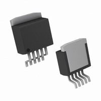
LM2575SX-5.0/NOPB National Semiconductor, LM2575SX-5.0/NOPB Datasheet - Page 21

LM2575SX-5.0/NOPB
Manufacturer Part Number
LM2575SX-5.0/NOPB
Description
IC REG SW 5V 1A STP DN TO-263-5
Manufacturer
National Semiconductor
Series
SIMPLE SWITCHER®r
Type
Step-Down (Buck)r
Datasheet
1.LM2575S-5.0NOPB.pdf
(28 pages)
Specifications of LM2575SX-5.0/NOPB
Internal Switch(s)
Yes
Synchronous Rectifier
No
Number Of Outputs
1
Voltage - Output
5V
Current - Output
1A
Frequency - Switching
52kHz
Voltage - Input
4 ~ 40 V
Operating Temperature
-40°C ~ 125°C
Mounting Type
Surface Mount
Package / Case
D²Pak, TO-263 (5 leads + tab)
Lead Free Status / RoHS Status
Lead free / RoHS Compliant
Power - Output
-
Other names
*LM2575SX-5.0
*LM2575SX-5.0/NOPB
LM2575SX-5.0
*LM2575SX-5.0/NOPB
LM2575SX-5.0
Available stocks
Company
Part Number
Manufacturer
Quantity
Price
Part Number:
LM2575SX-5.0/NOPB
Manufacturer:
TI/德州仪器
Quantity:
20 000
NEGATIVE BOOST REGULATOR
Another variation on the buck-boost topology is the negative
boost configuration. The circuit in Figure 11 accepts an input
voltage ranging from −5V to −12V and provides a regulated
−12V output. Input voltages greater than −12V will cause the
output to rise above −12V, but will not damage the regulator.
Because of the boosting function of this type of regulator, the
switch current is relatively high, especially at low input volt-
ages. Output load current limitations are a result of the max-
imum current rating of the switch. Also, boost regulators can
not provide current limiting load protection in the event of a
shorted load, so some other means (such as a fuse) may be
necessary.
Typical Load Current
200 mA for V
500 mA for V
Note: Pin numbers are for TO-220 package.
UNDERVOLTAGE LOCKOUT
In some applications it is desirable to keep the regulator off
until the input voltage reaches a certain threshold. An under-
voltage lockout circuit which accomplishes this task is shown
in Figure 12, while Figure 13 shows the same circuit applied
to a buck-boost configuration. These circuits keep the regu-
lator off until the input voltage reaches a predetermined level.
DELAYED STARTUP
The ON /OFF pin can be used to provide a delayed startup
feature as shown in Figure 14. With an input voltage of 20V
and for the part values shown, the circuit provides approxi-
mately 10 ms of delay time before the circuit begins switching.
Increasing the RC time constant can provide longer delay
times. But excessively large RC time constants can cause
problems with input voltages that are high in 60 Hz or 120 Hz
ripple, by coupling the ripple into the ON /OFF pin.
ADJUSTABLE OUTPUT, LOW-RIPPLE
POWER SUPPLY
A 1A power supply that features an adjustable output voltage
is shown in Figure 15. An additional L-C filter that reduces the
output ripple by a factor of 10 or more is included in this circuit.
IN
IN
= −5.2V
= −7V
FIGURE 11. Negative Boost
V
TH
V
Z1
+ 2V
BE
(Q1)
1147516
21
Note: Complete circuit not shown.
Note: Pin numbers are for the TO-220 package.
Note: Complete circuit not shown (see Figure 10).
Note: Pin numbers are for the TO-220 package.
Note: Complete circuit not shown.
Note: Pin numbers are for the TO-220 package.
FIGURE 12. Undervoltage Lockout for Buck Circuit
FIGURE 13. Undervoltage Lockout
FIGURE 14. Delayed Startup
for Buck-Boost Circuit
1147519
www.national.com
1147517
1147518


