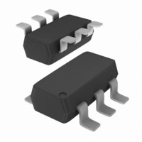
MAX1720EUTG ON Semiconductor, MAX1720EUTG Datasheet - Page 5

MAX1720EUTG
Manufacturer Part Number
MAX1720EUTG
Description
IC INVERTER CHRG PUMP VOLT 6TSOP
Manufacturer
ON Semiconductor
Type
Switched Capacitor (Charge Pump), Invertingr
Datasheet
1.MAX1720EUTG.pdf
(18 pages)
Specifications of MAX1720EUTG
Internal Switch(s)
Yes
Synchronous Rectifier
No
Number Of Outputs
1
Voltage - Output
-1.5 ~ -5.5 V, 3 ~ 11 V
Current - Output
50mA
Frequency - Switching
12kHz
Voltage - Input
1.5 ~ 5.5 V
Operating Temperature
-40°C ~ 85°C
Mounting Type
Surface Mount
Package / Case
SC-74-6
Power - Output
313mW
Function
Inverting
Output Voltage
- 5.5 V to - 1.15 V
Output Current
100 mA
Maximum Operating Temperature
+ 150 C
Mounting Style
SMD/SMT
Operating Supply Voltage (min)
1.15V
Operating Supply Voltage (max)
5.5V
Package Type
TSOP
Pin Count
6
Mounting
Surface Mount
Lead Free Status / RoHS Status
Lead free / RoHS Compliant
Other names
MAX1720EUTGOS
Available stocks
Company
Part Number
Manufacturer
Quantity
Price
Company:
Part Number:
MAX1720EUTG
Manufacturer:
ON Semiconductor
Quantity:
1 150
DETAILED OPERATING DESCRIPTION
applied to the V
operation (Figure 15). During the first phase, switches S
S
charges to the voltage on V
C
S
charge to C
APPLICATIONS INFORMATION
Output Voltage Considerations
provide regulation. The output voltage will drop in a linear
manner with respect to load current. The value of this
equivalent output resistance is approximately 26 W nominal
at 25°C with V
loads, and drops according to the equation below:
4
3
2
V
The MAX1720 charge pump converter inverts the voltage
The MAX1720 performs voltage conversion but does not
. During the second phase, S
Figure 15. Ideal Switched Capacitor Charge Pump
are open and S
V
are open. This action connects C
From Osc
in
in
Figure 14. Test Setup/Voltage Inverter
+
C
2
.
3
S1
S3
in
V out + * (V in * V DROP )
C
1
2
3
V DROP + I out
in
= 5.0 V. V
1
= C
1
pin. Conversion consists of a two−phase
C
and S
1
OSC
2
= C
3
out
in
3
S2
S4
are closed. During this time, C
= 10 mF
and load current is supplied from
is approximately −5.0 V at light
2
and S
6
5
4
R out
4
1
are closed, and S
C
across C
2
+
C
1
+
C
2
−V
2
, restoring
out
−V
out
http://onsemi.com
2
1
R
and
and
L
MAX1720
1
5
Charge Pump Efficiency
pump is affected by four factors:
These losses are given by Equation 1.
resistance of an ideal switched capacitor circuit (Figures 16
and 17).
Equation 2. The output voltage ripple is given by Equation 3.
P LOSS + [ 0.5C 1 (V in
The overall power conversion efficiency of the charge
Most of the conversion losses are due to factors 2, 3 and 4.
The 1/(f
The losses due to charge transfer above are also shown in
1. Losses from power consumed by the internal
2. I
3. Charge pump capacitor losses due to Equivalent
4. Losses that occur during charge transfer from the
V
V
(f
in
in
oscillator, switch drive, etc. (which vary with input
voltage, temperature and oscillator frequency).
switches on−board the charge pump.
Series Resistance (ESR).
commutation capacitor to the output capacitor when
a voltage difference between the two capacitors
exists.
P
V
OSC
Figure 16. Ideal Switched Capacitor Model
2
LOSS(2,3,4)
Figure 17. Equivalent Output Resistance
R losses due to the on−resistance of the MOSFET
) 0.5C 2 (V RIPPLE
RIPPLE
R
1
OSC
EQUIV
)C 1
)(C
) 8R
R
1
+
+
) term in Equation 1 is the effective output
f
EQUIV
(f
f
C
+ I out
OSC
SWITCH
1
1
C 1
2
I out
* V out
)(C 2 )
2
2
* 2V out V RIPPLE )]
) 4ESR
) 2(I out )(ESR
R out ^ I out
2
)
C
C
C 1
2
2
) ESR
2
R
R
C 2
L
L
)
V
V
C 2
(eq. 3)
out
out
f OSC
(eq. 2)
(eq. 1)


