LM2596DSADJR4G ON Semiconductor, LM2596DSADJR4G Datasheet - Page 3
LM2596DSADJR4G
Manufacturer Part Number
LM2596DSADJR4G
Description
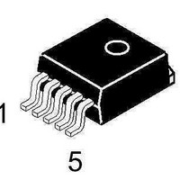
IC REG SW STP-DWN 3A D2PAK-5
Manufacturer
ON Semiconductor
Type
Step-Down (Buck)r
Datasheet
1.LM2596DSADJR4G.pdf
(25 pages)
Specifications of LM2596DSADJR4G
Internal Switch(s)
Yes
Synchronous Rectifier
No
Number Of Outputs
1
Voltage - Output
1.23 ~ 37 V
Current - Output
3A
Frequency - Switching
150kHz
Voltage - Input
4.5 ~ 40 V
Operating Temperature
-40°C ~ 125°C
Mounting Type
Surface Mount
Package / Case
D²Pak, TO-263 (5 leads + tab)
Output Voltage
1.23 V to 37 V
Output Current
3 A
Input Voltage
- 5 V to - 12 V
Switching Frequency
150 KHz
Operating Temperature Range
- 40 C to + 125 C
Mounting Style
SMD/SMT
Duty Cycle (max)
95 %
Lead Free Status / RoHS Status
Lead free / RoHS Compliant
Power - Output
-
Lead Free Status / Rohs Status
Lead free / RoHS Compliant
Available stocks
Company
Part Number
Manufacturer
Quantity
Price
Company:

Part Number:
LM2596DSADJR4G
Manufacturer:
ON
Quantity:
12 400
Part Number:
LM2596DSADJR4G
Manufacturer:
ON/安森美
Quantity:
20 000


PIN FUNCTION DESCRIPTION
OPERATING RATINGS
specific performance limits. For guaranteed specifications and test conditions, see the Electrical Characteristics.)
Pin
Operating Junction Temperature Range
Supply Voltage
1
2
3
4
5
Feedback
ON/OFF
Symbol
Output
GND
V
in
This pin is the positive input supply for the LM2596 step−down switching regulator. In order to minimize voltage transi-
ents and to supply the switching currents needed by the regulator, a suitable input bypass capacitor must be present
(C
This is the emitter of the internal switch. The saturation voltage V
kept in mind that the PCB area connected to this pin should be kept to a minimum in order to minimize coupling to
sensitive circuitry.
Circuit ground pin. See the information about the printed circuit board layout.
This pin is the direct input of the error amplifier and the resistor network R2, R1 is connected externally to allow pro-
gramming of the output voltage.
It allows the switching regulator circuit to be shut down using logic level signals, thus dropping the total input supply
current to approximately 80 mA. The threshold voltage is typically 1.6 V. Applying a voltage above this value (up to
+V
will be in the “on” condition.
in
in
) shuts the regulator off. If the voltage applied to this pin is lower than 1.6 V or if this pin is left open, the regulator
in Figure 1).
(Operating Ratings indicate conditions for which the device is intended to be functional, but do not guarantee
Rating
http://onsemi.com
Description (Refer to Figure 1)
3
sat
of this output switch is typically 1.5 V. It should be
Symbol
V
T
in
J
−40 to +125
4.5 to 40
Value
Unit
°C
V
Related parts for LM2596DSADJR4G
Image
Part Number
Description
Manufacturer
Datasheet
Request
R

Part Number:
Description:
Simple Switcher Power Converter 150 KHZ 3A Step-down Voltage Regulator, Package: to 263, Pin Nb=5
Manufacturer:
National Semiconductor

Part Number:
Description:
ON Semiconductor [VOLTAGE REGULATOR]
Manufacturer:
ON Semiconductor
Datasheet:
Part Number:
Description:
357-036-542-201 CARDEDGE 36POS DL .156 BLK LOPRO
Manufacturer:
ON Semiconductor
Datasheet:
Part Number:
Description:
357-036-542-201 CARDEDGE 36POS DL .156 BLK LOPRO
Manufacturer:
ON Semiconductor
Datasheet:
Part Number:
Description:
357-036-542-201 CARDEDGE 36POS DL .156 BLK LOPRO
Manufacturer:
ON Semiconductor
Datasheet:
Part Number:
Description:
357-036-542-201 CARDEDGE 36POS DL .156 BLK LOPRO
Manufacturer:
ON Semiconductor
Datasheet:
Part Number:
Description:
357-036-542-201 CARDEDGE 36POS DL .156 BLK LOPRO
Manufacturer:
ON Semiconductor
Datasheet:
Part Number:
Description:
357-036-542-201 CARDEDGE 36POS DL .156 BLK LOPRO
Manufacturer:
ON Semiconductor
Datasheet:
Part Number:
Description:
357-036-542-201 CARDEDGE 36POS DL .156 BLK LOPRO
Manufacturer:
ON Semiconductor
Datasheet:
Part Number:
Description:
357-036-542-201 CARDEDGE 36POS DL .156 BLK LOPRO
Manufacturer:
ON Semiconductor
Datasheet:
Part Number:
Description:
357-036-542-201 CARDEDGE 36POS DL .156 BLK LOPRO
Manufacturer:
ON Semiconductor
Datasheet:
Part Number:
Description:
357-036-542-201 CARDEDGE 36POS DL .156 BLK LOPRO
Manufacturer:
ON Semiconductor
Datasheet:
Part Number:
Description:
Manufacturer:
ON Semiconductor
Datasheet:
Part Number:
Description:
Manufacturer:
ON Semiconductor
Datasheet: