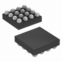
MAX8649EWE+T Maxim Integrated Products, MAX8649EWE+T Datasheet - Page 10

MAX8649EWE+T
Manufacturer Part Number
MAX8649EWE+T
Description
IC REG STEP-DOWN 1.8A 16-WLP
Manufacturer
Maxim Integrated Products
Type
Step-Down (Buck)r
Datasheet
1.MAX8649EWET.pdf
(32 pages)
Specifications of MAX8649EWE+T
Internal Switch(s)
Yes
Synchronous Rectifier
Yes
Number Of Outputs
1
Voltage - Output
0.75 ~ 1.38 V
Current - Output
1.8A
Frequency - Switching
3.25MHz
Voltage - Input
2.5 ~ 5.5 V
Operating Temperature
-40°C ~ 85°C
Mounting Type
Surface Mount
Package / Case
16-WLP
Power - Output
1.04W
Lead Free Status / RoHS Status
Lead free / RoHS Compliant
1.8A Step-Down Regulator with Differential
Remote Sense in 2mm x 2mm WLP
10
C3, C4
B3, B4
BUMP
______________________________________________________________________________________
C1
C2
D1
D2
D3
D4
A1
A2
A3
A4
B1
B2
NAME
AGND
PGND
SNS+
SYNC
VID1
SNS-
VID0
SDA
V
SCL
IN1
IN2
EN
LX
DD
Anal og S up p l y V ol tag e Inp ut. The i np ut vol tag e r ang e i s 2.5V to 5.5V . Place an 11Ω resistor between
IN1 and the input supply. Bypass the input supply with a 2.2µF ceramic capacitor as close as
possible to the 11Ω resistor. Byp ass IN 1 to the 2.2µF cap aci tor g r ound p l ane ter m i nal w i th a 0.1µF
cer am i c cap aci tor as cl ose as p ossi b l e to the IC . C onnect IN 1 and IN 2 to the sam e p ow er sour ce.
Analog Ground. Connect AGND to the PCB ground plane.
Voltage ID Control Input. The logic states of VID0 and VID1 select the register that sets the output
voltage.
Power-Supply Voltage Input. The input voltage range is from 2.5V to 5.5V. IN2 powers the internal
p-channel and n-channel MOSFETs. Bypass IN2 to PGND with 10µF and 0.1µF ceramic capacitors
as close as possible to the IC. Connect IN1 and IN2 to the same power source.
Output Voltage Remote Sense, Positive Input. Connect SNS+ directly to the output at the load.
Logic Enable Input. Drive EN high to enable the DC-DC step-down regulator, or low to place in
shutdown mode. In shutdown mode, this logic input has an internal pulldown resistor to AGND.
Inductor Connection. LX is connected to the drains of the internal p-channel and n-channel
MOSFETs. LX is high impedance during shutdown.
Output Voltage Remote Sense, Negative Input. Connect to a quiet ground directly at the load.
Voltage ID Control Input. The logic states of VID0 and VID1 select the register that sets the output
voltage.
Power Ground. Connect both PGND bumps to the PCB ground plane.
Logic Input Supply Voltage. Connect V
V
registers are reset, but the EN control is still active in this mode.
I
I
E xter nal C l ock S ynchr oni zati on Inp ut. C onnect S Y N C to a 13M H z, 19.2M H z, or 26M H z system cl ock.
The D C - D C r eg ul ator can b e for ced to synchr oni ze to thi s exter nal cl ock d ep end i ng on I
Tab l e 8. S Y N C d oes not have an i nter nal p ul l d ow n. C onnect S Y N C to AG N D i f not used .
2
2
DD
C D ata Inp ut. D ata i s r ead on the r i si ng ed g e of S C L and d ata i s cl ocked out on the fal l i ng ed g e of S C L.
C Clock Input
to AGND with a 0.1µF ceramic capacitor. When V
DD
to the logic supply driving SDA, SCL, and SYNC. Bypass
FUNCTION
DD
drops below the UVLO threshold, the I
Bump Description
2
C setti ng . S ee
2
C


