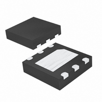
MAX8569BETT+T Maxim Integrated Products, MAX8569BETT+T Datasheet - Page 7

MAX8569BETT+T
Manufacturer Part Number
MAX8569BETT+T
Description
IC DC-DC CONV 200MA 6-TDFN
Manufacturer
Maxim Integrated Products
Type
Step-Up (Boost)r
Datasheet
1.MAX8569AETTT.pdf
(11 pages)
Specifications of MAX8569BETT+T
Internal Switch(s)
Yes
Synchronous Rectifier
Yes
Number Of Outputs
1
Voltage - Output
3.3V
Current - Output
200mA
Voltage - Input
1.5 ~ 5.5 V
Operating Temperature
-40°C ~ 85°C
Mounting Type
Surface Mount
Package / Case
6-TDFN Exposed Pad
Power - Output
1.45W
Lead Free Status / RoHS Status
Lead free / RoHS Compliant
Frequency - Switching
-
Lead Free Status / Rohs Status
Lead free / RoHS Compliant
The MAX8569A and MAX8569B compact high-efficien-
cy step-up converters feature low-quiescent supply cur-
rent to ensure the highest possible efficiency over a
wide load range. With a minimum 1.5V input voltage,
these devices are well suited for applications with two
alkaline cells, two nickel-metal-hydride (NiMH) cells, or
one lithium-ion (Li+) cell. When SHDN is low, the output
is connected to the battery through the inductor and an
internal p-channel MOSFET. This allows the input bat-
tery to be used as a backup or real-time clock supply
when the converter is off by eliminating the voltage drop
across the MOSFET body diode. These devices are
ideal for low-power applications where a small footprint
is critical. The internal synchronous rectifier improves
efficiency significantly and reduces size and cost by
eliminating the need for an external Schottky diode.
The MAX8569A/MAX8569B feature a current-limited
control scheme that provides ultra-low quiescent current
and high efficiency over a wide output current range.
The switching cycles are not controlled by an oscillator.
Figure 1. Typical Application Circuit for MAX8569A
Figure 2. Typical Application Circuit for MAX8569B
1.5V TO 3V
_______________________________________________________________________________________
INPUT
Detailed Description
10µF
1.5V TO 3V
C1
INPUT
200mA Step-Up Converters in 6-Pin
10µF
220kΩ
1MΩ
C1
Control Scheme
R1
R2
OFF
0.01µF
10µH
L1
10µH
C2
L1
ON
2
4
1
2
4
1
BATT
LX
SHDN
BATT
LX
SHDN
MAX8569B
MAX8569A
GND
Instead, switch on-time is terminated when the inductor
current reaches the 780mA (typ) n-channel current limit,
or when the 5µs maximum n-channel switch on-time is
reached. Following each on-cycle, the synchronous rec-
tifier turns on, shunts the MOSFET body diode, and the
inductor current ramps to zero before another cycle
begins. The next cycle occurs when the error compara-
tor senses that the output has fallen below the regulation
threshold.
Drive SHDN low to shut down the MAX8569A/
MAX8569B and reduce the input current to less than
1µA. During shutdown, the battery input is connected
to the output through the inductor and the internal syn-
chronous rectifier. This allows the input battery (rather
than a separate backup battery) to provide backup
power for devices such as an idled microcontroller,
SRAM, or real-time clock, without the usual diode for-
ward drop. Drive SHDN to V
the IC for normal operation.
GND
3
3
OUT
RST
OUT
FB
5
6
5
6
C3
22µF
SOT23 and TDFN
R3
168kΩ
R4
100kΩ
Applications Information
R1
100kΩ
C3
22µF
3.3V
OUTPUT
RESET
OUTPUT
3.3V OUTPUT
OUT
(logic-high) to enable
Shutdown
7


