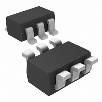
MAX8640YEXT25+T Maxim Integrated Products, MAX8640YEXT25+T Datasheet - Page 8

MAX8640YEXT25+T
Manufacturer Part Number
MAX8640YEXT25+T
Description
IC DC-DC CONV 2.5V SC70-6
Manufacturer
Maxim Integrated Products
Type
Step-Down (Buck)r
Datasheet
1.MAX8640YEXT12T.pdf
(12 pages)
Specifications of MAX8640YEXT25+T
Internal Switch(s)
Yes
Synchronous Rectifier
Yes
Number Of Outputs
1
Voltage - Output
2.5V
Current - Output
500mA
Frequency - Switching
2MHz
Voltage - Input
2.7 ~ 5.5 V
Operating Temperature
-40°C ~ 85°C
Mounting Type
Surface Mount
Package / Case
SC-70-6, SC-88, SOT-363
Power - Output
245mW
Lead Free Status / RoHS Status
Lead free / RoHS Compliant
* Contact factory for availability of each version. For 2.85V output
(82 version), request application note that includes limitations
and typical operating characteristics.
+ Denotes a lead(Pb)-free/RoHS-compliant package.
T = Tape and reel.
Note: All devices are specified over the -40°C to +85°C
operating temperature range.
Tiny 500mA, 4MHz/2MHz Synchronous
Step-Down DC-DC Converters
8
MAX8640ZEXT08+T
MAX8640YEXT24+T
MAX8640YEXT25+T
MAX8640YELT08+T
MAX8640YELT11+T
MAX8640YELT12+T
MAX8640YELT13+T
MAX8640YELT15+T
MAX8640YELT16+T
MAX8640YELT18+T
MAX8640YELT19+T
MAX8640YELT25+T
MAX8640YELT82+T
MAX8640ZEXT11+T
MAX8640ZEXT12+T
MAX8640ZEXT13+T
MAX8640ZEXT15+T
MAX8640ZEXT18+T
MAX8640ZELT08+T
MAX8640ZELT11+T
MAX8640ZELT12+T
MAX8640ZELT13+T
MAX8640ZELT15+T
MAX8640ZELT18+T
Ordering Information (continued)
_______________________________________________________________________________________
MAX8640ZELT12
MAX8640ZELT13
MAX8640ZELT15
MAX8640ZELT18
PART*
PART
VOLTAGE (V)
6 µDFN
PIN-
PACKAGE
6 SC70
6 SC70
6 µDFN
6 µDFN
6 µDFN
6 µDFN
6 µDFN
6 µDFN
6 µDFN
6 µDFN
6 µDFN
6 SC70
6 SC70
6 SC70
6 SC70
6 SC70
6 SC70
6 µDFN
6 µDFN
6 µDFN
6 µDFN
6 µDFN
6 µDFN
OUTPUT
1.2
1.3
1.5
1.8
FREQUENCY
TOP MARK
(MHz)
ADM
ACM
ACO
ACN
ACU
ACJ
ACL
ACP
3.6
3.7
3.9
4.0
OW
NG
NM
NO
NB
NC
ND
NE
NH
NK
NN
NP
NF
NJ
NL
NI
typically perform well. Due to the MAX8640Y/
MAX8640Z soft-start, the input capacitance can be very
low. For optimum noise immunity and low input ripple,
choose a capacitor value in µF that is equal to or larger
than the inductor’s value in µH.
High switching frequencies and large peak currents
make PCB layout a very important part of design. Good
design minimizes excessive EMI on the feedback paths
and voltage gradients in the ground plane, both of
which can result in instability or regulation errors.
Connect the inductor, input capacitor, and output
capacitor as close together as possible, and keep their
traces short, direct, and wide. Connect the two GND
pins under the IC and directly to the grounds of the
input and output capacitors. Keep noisy traces, such
as the LX node, as short as possible. Refer to the
MAX8640Z evaluation kit for an example PCB layout
and routing scheme.
PROCESS: BiCMOS
RECOMMENDED COMPONENTS
L1 (µH)
1
1
1
1
Selector Guide (continued)
PCB Layout and Routing
C2 (µF)
Chip Information
2.2
2.2
2.2
2.2
TOP MARK
NM
NO
NN
NP


