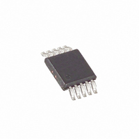
MAX868EUB+T Maxim Integrated Products, MAX868EUB+T Datasheet - Page 5

MAX868EUB+T
Manufacturer Part Number
MAX868EUB+T
Description
IC CHARGE PUMP INV 10-UMAX
Manufacturer
Maxim Integrated Products
Type
Switched Capacitor (Charge Pump), Doubler, Invertingr
Datasheet
1.MAX868EUB.pdf
(12 pages)
Specifications of MAX868EUB+T
Internal Switch(s)
Yes
Synchronous Rectifier
No
Number Of Outputs
1
Voltage - Output
-3.6 ~ -11 V
Current - Output
30mA
Frequency - Switching
450kHz
Voltage - Input
1.8 ~ 5.5 V
Operating Temperature
-40°C ~ 85°C
Mounting Type
Surface Mount
Package / Case
10-MSOP, Micro10™, 10-uMAX, 10-uSOP
Power - Output
444mW
Function
Inverting
Output Voltage
- 3.6 V to - 11 V
Output Current
30 mA
Maximum Operating Temperature
+ 85 C
Minimum Operating Temperature
- 40 C
Mounting Style
SMD/SMT
Lead Free Status / RoHS Status
Lead free / RoHS Compliant
The MAX868 inverting charge pump uses pulse-
frequency-modulation (PFM) control to generate a reg-
ulated negative output voltage up to -2 x V
operation is obtained by enabling the internal 450kHz
oscillator as needed to maintain output voltage regula-
tion. This control scheme reduces supply current at
light loads and permits the use of small capacitors.
The functional diagram shown in Figure 1 indicates the
two phases of MAX868 operation: charge phase ( 1)
and discharge phase ( 2). In charge phase, the
switches on the left-hand side close, and the switches
on the right-hand side open. In the discharge phase,
the inverse occurs.
Figure 2 illustrates that in charge phase, both flying
capacitors are charged in parallel. The load is serviced
entirely by the charge stored in the output capacitor.
Figure 3 demonstrates the series connection of the fly-
ing capacitors in the discharge phase. The series com-
bination of the flying capacitors, when connected to the
output capacitor, transfers charge to the output in order
to maintain output voltage regulation. In normal opera-
tion, the MAX868 operates predominantly in charge
phase, switching to discharge phase only as needed to
maintain a regulated output.
PIN
10
1
2
3
4
5
6
7
8
9
NAME
PGND
SHDN
GND
OUT
C1+
C2+
C1-
C2-
FB
IN
_______________________________________________________________________________________
Analog Ground
Charge-Pump Output
Negative Terminal of Flying Capacitor C1
Power Ground
Positive Terminal of Flying Capacitor C1
Negative Terminal of Flying Capacitor C2
Supply-Voltage Input. Input voltage range is 1.8V to 5.5V.
Positive Terminal of Flying Capacitor C2
Active-Low Shutdown Input. Connect SHDN to GND to put the MAX868 in shutdown mode and reduce sup-
ply current to 0.1µA. Connect to IN for normal operation. OUT is actively pulled to GND in shutdown.
Feedback Input. Connect FB to a resistor divider for a regulated output voltage. Connect to IN to generate
an unregulated -2 x V
Detailed Description
IN
output voltage.
IN
. PFM
Regulated, Adjustable -2x
Inverting Charge Pump
Figure 1. Functional Diagram
SHDN
FUNCTION
IN
OSCILLATOR
1
C2+
C1+
C2-
C1-
2
Pin Description
FB
V
REF
C
OUT
OUT
5


