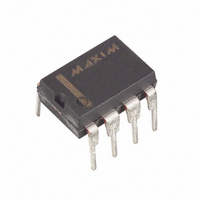
MAX1822EPA+ Maxim Integrated Products, MAX1822EPA+ Datasheet - Page 5

MAX1822EPA+
Manufacturer Part Number
MAX1822EPA+
Description
IC POWER SUPPLY HI SIDE 8-DIP
Manufacturer
Maxim Integrated Products
Type
Switched Capacitor (Charge Pump)r
Datasheet
1.MAX1822ESAT.pdf
(10 pages)
Specifications of MAX1822EPA+
Internal Switch(s)
Yes
Synchronous Rectifier
No
Number Of Outputs
1
Voltage - Output
14.5 ~ 27.5 V
Current - Output
25mA
Frequency - Switching
90kHz
Voltage - Input
3.5 ~ 16.5 V
Operating Temperature
-40°C ~ 85°C
Mounting Type
Through Hole
Package / Case
8-DIP (0.300", 7.62mm)
Lead Free Status / RoHS Status
Lead free / RoHS Compliant
Power - Output
-
Figure 1. MAX1822 Block Diagram
The MAX1822 is a multistage charge-pump power sup-
ply. Although the charge pump is capable of multiply-
ing V
+ 11V by an internal feedback circuit for inputs above
4V. The charge pump typically operates at 90kHz, but
regulates by pulse skipping. When V
+ 11V, the oscillator shuts off. As V
+ 11V, the oscillator turns on.
The Power-Ready Output (PR) signals control circuitry
when the high-side voltage reaches a preset level. This
feature can be used to protect external FET switches
from excess dissipation and damage by preventing them
from turning on, except when adequate gate drive levels
are present. When power is applied, PR remains low until
C1
(SWITCHES SHOWN IN REFRESH MODE)
CC
C3
TWO-STAGE CHARGE PUMP
V
S4
S3
S2
S1
up to four times, the output is regulated to V
INT
S8
S7
S6
S5
_______________________________________________________________________________________
Detailed Description
Charge-Pump Operation
C2
Power-Ready Output
OUT
OUT
CONTROL LOGIC
RC OSCILLATOR
dips below V
exceeds V
+
CC
CC
CC
OVERVOLTAGE
COMPARATOR
High-Side Power Supply
low if V
the output is overloaded. The PR high level is V
MAX1822 quiescent supply current varies with V
with the values of C1, C2, and C3 (Typical Operating
Characteristics). Even with no external load, the device
must still pump to overcome internal losses. Large ratios
between C3 and C1 or C2 require more charge-pump
cycles to restore V
current rises fairly rapidly to about 1mA at 4V (Typical
Operating Characteristics). This rise occurs because
V
ages; the oscillator runs continuously, so supply current
is higher. Figure 2 shows the test circuit for the
MAX1822 quiescent supply current.
V
OUT
OUT
no longer pulse skips to regulate at low input volt-
reaches approximately V
11V
OUT
falls below this level during operation, i.e., if
Applications Information
OUT
8.5V
. As V
Quiescent Supply Current
CC
POWER-READY
COMPARATOR
CC
falls below 5V, quiescent
+ 8.5V. PR also goes
PR DRIVER
CC
.
CC
V
V
PR
GND
OUT
CC
and
5


