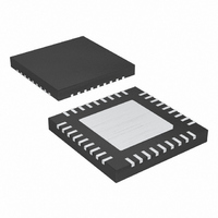
MAX15017BATX+T Maxim Integrated Products, MAX15017BATX+T Datasheet - Page 19

MAX15017BATX+T
Manufacturer Part Number
MAX15017BATX+T
Description
IC DC/DC CONV 1A 36-TQFN-EP
Manufacturer
Maxim Integrated Products
Type
Step-Down (Buck)r
Datasheet
1.MAX15017AATX.pdf
(26 pages)
Specifications of MAX15017BATX+T
Internal Switch(s)
Yes
Synchronous Rectifier
Yes
Number Of Outputs
2
Voltage - Output
1.26 ~ 32 V
Current - Output
1A
Frequency - Switching
135kHz ~ 500kHz
Voltage - Input
7.5 ~ 40 V
Operating Temperature
-40°C ~ 125°C
Mounting Type
Surface Mount
Package / Case
36-TQFN Exposed Pad
Power - Output
2.1W
Lead Free Status / RoHS Status
Lead free / RoHS Compliant
The following equations define the power modulator:
The switching frequency is internally set at 500kHz for
MAX15015/MAX15017 and can vary from 400kHz to
600kHz when driven with an external SYNC signal. The
switching frequency is internally set at 135kHz for
MAX15014/MAX15016 and can vary from 100kHz to
200kHz when driven with an external sync signal. The
crossover frequency (fC), which is the frequency when
the closed-loop gain is equal to unity, should be set to
around 1/10 of the switching frequency or below.
The crossover frequency occurs above the LC double-
pole frequency, and the error amplifier must provide a
gain and phase bump to compensate for the rapid gain
and phase loss from the LC double pole, which exhibits
little damping.
This is accomplished by utilizing a Type 3 compensator
that introduces two zeroes and three poles into the con-
trol loop. The error amplifier has a low-frequency pole
(f
can be achieved.
The two zeroes are at:
and
and the higher frequency poles are at:
and
The compensation design primarily depends on the
type of output capacitor. Ceramic capacitors exhibit
very low ESR, and are well suited for high-switching-
frequency applications, but are limited in capacitance
P1
) near the origin so that tight voltage regulation at DC
1A, 4.5V to 40V Input Buck Converters with
G
f
f
LC
ZESR
MOD DC
f
f
P3
Z2
=
______________________________________________________________________________________
f
=
2
f
P2
=
ZI
=
_
× ×
2
2
2
=
=
π
π
π (
× ×
2
×
×
2
=
π
π
π
R
R
V
×
5
L C
×
1
3
RAMP
C
R
×
V
R
×
1
1
+
IN
1
1
OUT
5
6
C
C
1
R
×
×
7
7
OUT
6
C
C
)
×
+
=
×
7
×
6
C
C
10
ESR
C
8
8
6
50mA Auxiliary LDO Regulators
value and tend to be more expensive. Aluminum elec-
trolytic capacitors have much larger ESR but can reach
much larger capacitance values.
This is usually the case when a ceramic capacitor is
selected. In this case, f
shows the error amplifier feedback as well as its gain
response.
f
pensate for the gain and phase loss due to the double
pole. To achieve a 0dB crossover with -20dB/decade
slope, poles f
quency f
The values for R3 and R4 are already determined in the
Setting the Output Voltage section. The value of R3 is
also used in the following calculations.
Since f
be approximated as R3.
Now we can calculate C6 for zero f
Figure 3. Error Amplifier Compensation Circuit (Closed-Loop
and Error-Amplifier Gain Plot) for Ceramic Capacitors
Z1
is set to 0.5 to 0.8 x f
GAIN
(dB)
Z2
C
V
OUT
.
< f
C
P2
< f
Compensation when f
and f
C6
P2
C
R3
6
, then R3 >> R6, and R3 + R6 can
CLOSED-LOOP
GAIN
P3
=
R4
f
R6
Z1
2
are set above the crossover fre-
ZESR
LC
π
f
Z2
×
and f
REF
f
LC
1
f
occurs after f
C
×
Z2
R
R5
f
3
P2
EA
Z2
C8
is set to f
f
P3
:
C7
EA
GAIN
C
C
LC
. Figure 3
FREQUENCY
COMP
< f
to com-
ZESR
19


