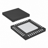
MAX15015BATX+T Maxim Integrated Products, MAX15015BATX+T Datasheet - Page 20

MAX15015BATX+T
Manufacturer Part Number
MAX15015BATX+T
Description
IC DC/DC CONV 1A 36-TQFN-EP
Manufacturer
Maxim Integrated Products
Type
Step-Down (Buck)r
Datasheet
1.MAX15017AATX.pdf
(26 pages)
Specifications of MAX15015BATX+T
Internal Switch(s)
Yes
Synchronous Rectifier
Yes
Number Of Outputs
2
Voltage - Output
1.26 ~ 32 V
Current - Output
1A
Frequency - Switching
135kHz ~ 500kHz
Voltage - Input
4.5 ~ 40 V
Operating Temperature
-40°C ~ 125°C
Mounting Type
Surface Mount
Package / Case
36-TQFN Exposed Pad
Power - Output
2.1W
Lead Free Status / RoHS Status
Lead free / RoHS Compliant
1A, 4.5V to 40V Input Buck Converters with
50mA Auxiliary LDO Regulators
f
pensator gain (G
Therefore, G
tor gain at f
Since G
The frequency of f
calculate C7:
f
then calculated by:
Note that if the crossover frequency has been chosen
as 1/10 of the switching frequency, then f
The purpose of f
switching ripple at the COMP pin.
If the ESR zero (f
f
way, the Bode plot of the loop gain plot will not flatten
out soon after the 0dB crossover, and will maintain
its -20dB/decade slope up to 1/2 of the switching
frequency.
If the ESR zero well exceeds f
should in any case be set high enough not to erode the
phase margin at the crossover frequency. For example,
it can be set between 5 x f
The value for C8 is calculated from:
For larger ESR capacitors such as tantalum and alu-
minum electrolytic, f
< f
remain the same as before however, f
set equal to f
20
C
P2
C
occurs between f
and f
C
is set at 1/2 the switching frequency (f
, then f
______________________________________________________________________________________
EA
SW
(f
C
C
C
/ 2, then f
G
EA
) x G
is:
MOD C
occurs between f
ZESR
(f
C
R
Compensation when f
C
EA
8
C
R
6
P3
) = 2π x f
MOD
Z1
( )
5
7
=
=
ZESR
f
) at f
. The output capacitor’s ESR zero
=
=
Z2
(
ZESR
is to further attenuate the residual
2
2
is set to 0.5 x f
P3
π
f
0 5 2
=
π
C
(f
C
and f
.
×
C
C
) occurs in a region between
×
(
× ×
2
6
can be used to cancel it. This
C
) = 1, R5 is calculated by:
×
C
is due primarily to C6 and R5.
L C
π
can occur before f
C
×
6
C
7
×
G
and 10 x f
π
×
P2
×
x C6 x R5 and the modula-
G
C
f
MOD DC
C
1
×
( .
1
R
MOD DC
0 5
. In this region, the com-
OUT
7
)
R
5
SW
P2
2
5
×
× ×
×
_
×
/2 (or even f
f
P
and f
L C
_
×
f
LC
f
SW
3
LC
2
−
π
C
and now we can
)
1
.
OUT
)
P3
P2
. f
C
= 5xf
Z1
P2
SW
C
> f
. If f
SW
). R6 is
and f
is now
C
ZESR
.
), f
ZESR
P3
Z2
frequency is higher than f
loop crossover frequency. The equations that define
the error amplifier’s poles and zeros (f
f
than the closed-loop crossover frequency. Figure 4
shows the error amplifier feedback as well as its gain
response for circuits that use higher-ESR output capac-
itors (tantalum or aluminum electrolytic).
Again, starting from R3, calculate C6 for zero f
and then place f
lated as:
If the value obtained here for R6 is not considerably
smaller than R3, then recalculate C6 using (R3 + R6) in
place of R3. Then use the new value of C6 to obtain a
better approximation for R6. The process can be further
iterated, and convergence is ensured as long as f
f
Figure 4. Error Amplifier Compensation Circuit (Closed-Loop
and Error-Amplifier Gain Plot) for Higher ESR Output
Capacitors
P3
ZESR
) are the same as before. However, f
GAIN
(dB)
.
V
OUT
C6
P2
R3
R4
to cancel the ESR zero. R6 is calcu-
R
C
R6
f
Z1
6
6
=
=
f
Z2
C
2
REF
LC
π
OUT
CLOSED-LOOP
GAIN
×
C
but lower than the closed-
f
LC
1
R5
6
×
f
P2
EA
ESR
×
C8
R
3
f
C
C7
f
P3
Z1
P2
, f
is now lower
FREQUENCY
COMP
Z2
, f
Z2
EA
GAIN
P2
:
, and
LC
<


