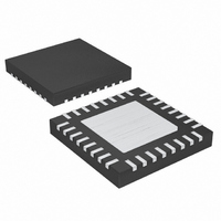
MAX5098AATJ+T Maxim Integrated Products, MAX5098AATJ+T Datasheet - Page 15

MAX5098AATJ+T
Manufacturer Part Number
MAX5098AATJ+T
Description
IC CONV BUCK/BOOST DL 32TQFN-EP
Manufacturer
Maxim Integrated Products
Type
Step-Down (Buck), Step-Up (Boost)r
Datasheet
1.MAX5098AATJ.pdf
(28 pages)
Specifications of MAX5098AATJ+T
Internal Switch(s)
Yes
Synchronous Rectifier
No
Number Of Outputs
2
Voltage - Output
0.8 ~ 0.85 V, 4.5 ~ 28 V
Current - Output
1A, 2A
Frequency - Switching
200kHz ~ 2.2MHz
Voltage - Input
4.5 ~ 19 V
Operating Temperature
-40°C ~ 125°C
Mounting Type
Surface Mount
Package / Case
32-TQFN Exposed Pad
Power - Output
2.76W
Lead Free Status / RoHS Status
Lead free / RoHS Compliant
The internal oscillator generates the 180° out-of-phase
clock signal required by each regulator. The switching
frequency of each converter (f
from 200kHz to 2.2MHz using a single 1% resistor at
R
With dual synchronized out-of-phase operation, the
MAX5098A’s internal MOSFETs turn on 180° out-of-
phase. The instantaneous input current peaks of both
regulators do not overlap, resulting in reduced RMS rip-
ple current and input-voltage ripple. This reduces the
required input capacitor ripple current rating, allows for
fewer or less expensive capacitors, and reduces
shielding requirements for EMI.
The main oscillator can be synchronized to the system
clock by applying an external clock (f
The f
ating frequency of an individual converter. Use a TTL
logic signal for the external clock with at least 100ns
pulse width. R
synchronization. Program the internal oscillator fre-
quency to have f
synchronized if the SYNC frequency, f
within ±20%.
Two MAX5098As can be connected in the master-slave
configuration for four ripple-phase operation (Figure 1).
The MAX5098A provides a clock output (CKO) that is
45° phase-shifted with respect to the internal switch
turn-on edge. Feed the CKO of the master to the SYNC
input of the slave. The effective input ripple switching
frequency is four times the individual converter’s switch-
ing frequency. When driving the master converter using
an external clock at SYNC, set the f
cycle to 50% for effective 90° phase-shifted interleaved
operation. When a SYNC is applied (and FSEL_1 = 0),
converter 1 duty cycle is limited to 75% (max).
All internal control circuitry operates from an internally
regulated nominal voltage of 5.2V (V
voltages (V+) of 5.2V to 19V, V
5.2V or below, the internal linear regulator operates in
dropout mode, where V
load on V
reduce V
threshold. Do not use V
For input voltages less than 5.5V, connect V+ and V
together. The load on V
frequency of converter 1 and converter 2. See the V
Internal Oscillator/Out-of-Phase Operation
OSC
SYNC
. See the Setting the Switching Frequency section.
L
L
, the dropout voltage can be high enough to
frequency must be twice the required oper-
below the undervoltage lockout (UVLO)
Converter with 80V Load-Dump Protection
OSC
SW
Internal Linear Regulator (V
Dual, 2.2MHz, Automotive Buck or Boost
______________________________________________________________________________________
is still required when using external
= 1/2 f
L
L
L
Synchronization (SYNC)/
to power external circuitry.
is proportional to the switching
follows V+. Depending on the
SYNC.
Clock Output (CKO)
L
Input Voltage (V+)/
is regulated to 5.2V. At
SW
The device is properly
) is programmable
L
SYNC
). At higher input
SYNC
SYNC
) at SYNC.
clock duty
, varies
L
L
L
)
Output Voltage vs. Converter Switching Frequency
graph in the Typical Operating Characteristics . For
input voltage ranges higher than 5.5V, disconnect V
from V+.
Bypass V+ to SGND with a 1µF or greater ceramic
capacitor placed close to the MAX5098A. Bypass V
with a 4.7µF ceramic capacitor to SGND.
The MAX5098A includes an undervoltage lockout with
hysteresis and a power-on-reset circuit for converter
turn-on and monotonic rise of the output voltage. The
falling UVLO threshold is internally set to 4.1V (typ) with
180mV hysteresis. Hysteresis at UVLO eliminates “chat-
tering” during startup. When V
internal MOSFET switches are turned off.
The MAX5098A digital soft-start reduces input inrush
currents and glitches at the input during turn-on. When
UVLO is cleared and EN_ is high, digital soft-start slow-
ly ramps up the internal reference voltage in 64 steps.
The total soft-start period is 4096 internal oscillator
switching cycles.
Driving EN_ low initiates digital soft-stop that slowly
ramps down the internal reference voltage in 64 steps.
The total soft-stop period is equal to the soft-start period.
To calculate the soft-start/soft-stop period, use the fol-
lowing equation:
where f
each converters’ switching frequency (FSEL_1 = V
The MAX5098A dual converter provides separate
enable inputs, EN1 and EN2, to individually control or
sequence the output voltages. These active-high enable
inputs are TTL compatible. Driving EN_ high initiates
soft-start of the converter, and PGOOD_ goes logic-high
when the converter output voltage reaches the
V
stop of the converter, and immediately forces PGOOD_
low. Use EN1, EN2, and PGOOD1 for sequencing (see
Figure 2). Connect PGOOD1 to EN2 to make sure con-
verter 1’s output is within regulation before converter 2
starts. Add an RC network from V
delay the individual converter. Sequencing reduces
input inrush current and possible chattering. Connect
EN_ to V
TPGOOD_
CKO
L
for always-on operation.
threshold. Driving EN_ low initiates a soft-
is the internal oscillator and f
t
SS
(
ms
)
=
Undervoltage Lockout/
f
CKO
L
Soft-Start/Soft-Stop
4096
Enable (EN1, EN2)
drops below UVLO, the
(
kHz
L
to EN1 and EN2 to
)
CKO
is twice
L
)
15
L
L


