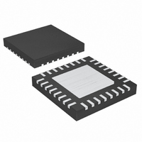
MAX5099ATJ+T Maxim Integrated Products, MAX5099ATJ+T Datasheet - Page 4

MAX5099ATJ+T
Manufacturer Part Number
MAX5099ATJ+T
Description
IC CONV BUCK SYNC DL 32TQFN-EP
Manufacturer
Maxim Integrated Products
Type
Step-Down (Buck)r
Datasheet
1.MAX5099ATJ.pdf
(27 pages)
Specifications of MAX5099ATJ+T
Internal Switch(s)
Both
Synchronous Rectifier
Yes
Number Of Outputs
2
Voltage - Output
0.8 ~ 17.1 V
Current - Output
1A, 2A
Frequency - Switching
200kHz ~ 2.2MHz
Voltage - Input
4.5 ~ 19 V
Operating Temperature
-40°C ~ 125°C
Mounting Type
Surface Mount
Package / Case
32-TQFN Exposed Pad
Power - Output
2.76W
Lead Free Status / RoHS Status
Lead free / RoHS Compliant
Dual, 2.2MHz, Automotive Synchronous Buck
Converter with 80V Load-Dump Protection
ELECTRICAL CHARACTERISTICS (continued)
(VDRV = V
C
T
4
On-Resistance High-Side
MOSFET Converter 2
Minimum Converter 1 Output
Current
Minimum Converter 2 Output
Current
Converter 1/Converter 2
MOSFET DRAIN_ Leakage
Current
Internal Weak Low-Side Switch
On-Resistance
INTERNAL SWITCH CURRENT LIMIT
Internal Switch Current-Limit
Converter 1
Internal Switch Current-Limit
Converter 2
SWITCHING FREQUENCY
PWM Maximum Duty Cycle
Switching Frequency Range
Switching Frequency
Switching Frequency Accuracy
SYNC Frequency Range
SYNC High Threshold
SYNC Low Threshold
SYNC Input Leakage
SYNC Input Minimum Pulse
Width
Sync to Source 1 Phase Delay
J
BYPASS
= -40°C to +125°C, unless otherwise noted.) (Note 2)
_______________________________________________________________________________________
= 0.22μF (low ESR), C
PARAMETER
L
, V+ = V
L
= IN_HIGH = 5.2V or V+ = IN_HIGH = 5.2V to 19V, EN_ = V
VL
= 4.7μF (ceramic), C
SYNC
I
R
SYNC_LEAK
SYMBOL
V
ONLSSW_
V
t
SYNCIN
I
I
D
f
R
I
SYNCH
SYNCL
OUT1
OUT2
SYNC
I
I
LK12
f
f
CL1
CL2
MAX
ON2
SW
SW
PHASE
I
V
I
V
V
V
V
19V, V
I
V+ = V
V
V+ = V
V
SYNC = SGND, f
R
5.6kΩ < R
10kΩ < R
Each converter switching frequency is half
of the SYNC input frequency,
FSEL_1 = V
Switching Frequency section)
R
SWITCH
SWITCH
LSSW
SOURCE2
SOURCE2
OUT1
OUT2
EN1
BST_
BST_
OSC
OSC
V+
= V
/V
/V
= 1μF (low ESR), C
= 6.81kΩ, each converter
= 62.5kΩ
= 30mA
SOURCE_
= 5V, V+ = 12V (Note 4)
= 3.3V, V+ = 12V (Note 4)
IN_HIGH
IN_HIGH
DD_
DD_
= 100mA, BST2/VDD2 to
= 100mA, BST2/VDD2 to
EN2
OSC
OSC
= 5.2V
= 4.5V
= 5.2V
L
= 5.2V
= 0V, V
(see the Setting the
< 62.5kΩ, 1%
CONDITIONS
< 10kΩ, 1%
= 5.2V, V
= 5.2V, V
= 0V
SW
= 1.25MHz
DS
= 19V, V
L
L
IN_HIGH
= VDRV =
= VDRV =
DRAIN_
= 1μF (ceramic), R
L
, SYNC = GND, I
=
MIN
1.75
200
400
2.8
1.7
90
2
IN_HIGH
VL
TYP
3.45
2.10
280
300
100
1.9
22
92
90
= 0mA, PGND = SGND,
2
1
5
7
= 3.9kΩ, R
MAX
2200
4400
2.60
520
100
4.3
2.1
0.8
20
2
OSC
Degrees
UNITS
= 10kΩ,
MHz
kHz
kHz
mΩ
μA
μA
ns
%
%
Ω
A
A
A
A
V
V


