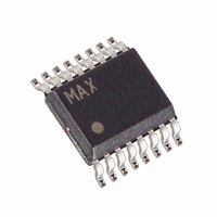
MAX686EEE Maxim Integrated Products, MAX686EEE Datasheet - Page 10

MAX686EEE
Manufacturer Part Number
MAX686EEE
Description
INVERT BOOST DAC-CONTROL 16QSOP
Manufacturer
Maxim Integrated Products
Type
Step-Up (Boost), Invertingr
Datasheet
1.MAX686EEE.pdf
(16 pages)
Specifications of MAX686EEE
Internal Switch(s)
Yes
Synchronous Rectifier
No
Number Of Outputs
1
Voltage - Output
±27.5V
Current - Output
100mA
Frequency - Switching
300kHz
Voltage - Input
2.7 ~ 5.5 V
Operating Temperature
-40°C ~ 85°C
Mounting Type
Surface Mount
Package / Case
16-QSOP
Power - Output
667mW
Lead Free Status / RoHS Status
Contains lead / RoHS non-compliant
Other names
Q1752000
Available stocks
Company
Part Number
Manufacturer
Quantity
Price
Part Number:
MAX686EEE
Manufacturer:
MAXIM/美信
Quantity:
20 000
Company:
Part Number:
MAX686EEE+
Manufacturer:
Maxim
Quantity:
675
DAC-Controlled Boost/Inverter
LCD Bias Supply with Internal Switch
POK is the input to the power-OK comparator. The
comparator drives an internal N-channel MOSFET. The
MOSFET’s open-drain output, LCDON, can drive an
external PNP transistor or P-channel MOSFET, switch-
ing a positive V
the voltage at POK exceeds 1.125V (power OK),
LCDON goes low, turning on the external PNP transis-
tor. When the voltage at POK drops below 1.125V
(power not OK), the external PNP transistor turns off,
cutting off power to the LCD display. This feature
ensures that the LCD display is not damaged due to
improper voltage levels. During shutdown or undervolt-
age lockout, LCDON is high impedance.
When SHDN is low, the MAX686 enters shutdown
mode, in which the control circuit, POK comparator,
DAC output buffer, reference, and internal biasing cir-
cuitry turn off. The DAC setting is stored as long as V
remains above the DAC reset threshold. Supply current
drops to 1.5µA. SHDN is a logic-level input; connect it
to V
The output voltage in shutdown mode depends on the
output voltage polarity. In the positive output voltage
configuration (Figure 1), the output is directly connect-
ed to the input through the diode (D1) and the inductor
(L1). When the device is in shutdown mode, the output
voltage falls to one diode drop below the input voltage,
and any load connected to the output may still conduct
current. In the negative output voltage configuration
(Figures 2 and 3), there is no DC path between the
input and the output, and the output falls to GND in
shutdown mode.
The MAX686 contains an internal 6-bit counter and
DAC to control the output voltage digitally (see the sec-
tion Setting the Output Voltage with the DAC ). The UP
and DN input pins drive an internal up/down counter
that directly controls the DAC. To increase the magni-
tude of V
edge to UP. This decreases the DAC output voltage
one step and correspondingly increases V
Conversely, to decrease the magnitude of V
a rising edge to DN. This increases the DAC output
voltage one step and correspondingly decreases
V
negative output to maintain the same control direction of
the absolute magnitude of the output voltage. Upon
power-up, the DAC code internally goes to mid-scale.
The DAC’s internal counter does not roll over once it
reaches full scale or zero. Therefore, additional rising
10
OUT
CC
______________________________________________________________________________________
. The UP and DN control direction reverses for a
for normal operation.
OUT
in the boost configuration, apply a rising
OUT
to the LCD (Figures 6 and 7). When
Power-OK Comparator
Shutdown Mode
Internal DAC
OUT
, apply
OUT.
CC
edges to make the counter roll over are ignored, pre-
venting unexpected undervoltages or overvoltages.
The MAX626’s 1.25V internal reference is accurate to
±2% over temperature. It can source up to 50µA of cur-
rent and should be bypassed with at least a 0.1µF
capacitor. See the Bypass Capacitors section.
For either positive or negative output voltage applica-
tions, set the MAX686’s output voltage using three exter-
nal resistors (R1, R2, and R3) as shown in Figures 1, 2,
and 3. Since the input bias current at FB has a 50nA
maximum value, large resistors can be used in the
feedback loop without a significant loss of accuracy.
Select R1 to be in the 10k
late R2 and R3 using the applicable equations from the
following subsections.
The minimum output voltage is set with the resistor-
divider (R1-R2, Figure 1) from V
mum output voltage occurs when V
1.25V. Therefore, R3 has no effect on the minimum out-
put voltage. Choose R1 to be 120k
in the divider is about 10µA. Then determine R2 as fol-
lows:
For example, if V
Mount R1 and R2 close to the FB pin to minimize para-
sitic capacitance.
The DAC is adjustable from 0V to 1.25V in 64 steps,
and 1LSB = 1.25V / 63 = 19.8mV. Calculate R3 to
adjust V
For V
mine R3 as follows:
The general form for V
put (V
At power-up, the DAC resets to mid-scale where
V
power-up is:
DACOUT
Setting the Output Voltage with the DAC
V
OUT
R2 = 120k x (12.5 - 1.25) / (1.25) =1.08M
OUT(MAX)
DACOUT
R3 = R2 x (V
V
Setting the Maximum Positive Output Voltage
Setting the Minimum Positive Output Voltage
OUT
OUT(MID)
= V
= 1.08M x (1.25) / (25 - 12.5) = 108k
= 0.635V. Therefore, the output voltage after
R2 = R1 x (V
with DACOUT (Figure 1).
OUT(MIN)
) is:
= 25V and V
OUT(MIN)
= V
FB
R2 / R3 = 18.65V
OUT(MIN)
) / (V
OUT
+ (V
OUT(MIN)
= 12.5V:
OUT(MAX
as a function of the DAC out-
Design Procedure
FB
to 220kΩ range and calcu-
OUT(MIN)
- V
+ (1.25 - 0.635) x
Internal Reference
DACOUT
- V
OUT
) - V
FB
so that the current
DACOUT
) / V
to FB. The mini-
OUT(MIN)
= 12.5V, deter-
) x R2 / R3
FB
= V
)
FB
=


