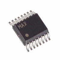
MAX1763EEE Maxim Integrated Products, MAX1763EEE Datasheet - Page 14

MAX1763EEE
Manufacturer Part Number
MAX1763EEE
Description
IC CONV DC/DC STEP UP LN 16QSOP
Manufacturer
Maxim Integrated Products
Type
Step-Up (Boost)r
Datasheet
1.MAX1763EEE.pdf
(16 pages)
Specifications of MAX1763EEE
Internal Switch(s)
Yes
Synchronous Rectifier
Yes
Number Of Outputs
1
Voltage - Output
3.3V, 2.5 ~ 5.5 V
Current - Output
1.5A
Frequency - Switching
1MHz
Voltage - Input
0.7 ~ 5.5 V
Operating Temperature
-40°C ~ 85°C
Mounting Type
Surface Mount
Package / Case
16-QSOP
Power - Output
667mW
Output Voltage
3.3 V
Output Current
1.5 A
Input Voltage
0.7 V to 5.5 V
Supply Current
2.5 mA
Switching Frequency
1200 MHz
Mounting Style
SMD/SMT
Maximum Operating Temperature
+ 85 C
Minimum Operating Temperature
- 40 C
Lead Free Status / RoHS Status
Contains lead / RoHS non-compliant
Available stocks
Company
Part Number
Manufacturer
Quantity
Price
Part Number:
MAX1763EEE
Manufacturer:
MAXIM/美信
Quantity:
20 000
electrolytic capacitors; their high ESR typically results
in higher output ripple voltage.
A few ceramic bypass capacitors are required for prop-
er operation. Bypass REF to GND with 0.22µF. Also,
bypass OUT to GND with a 1µF ceramic capacitor, and
connect OUT to POUT with a 4.7Ω resistor. Each of
these components should be placed as close to their
respective IC pins as possible, within 0.2in (5mm).
Table 5 lists suggested suppliers.
High switching frequencies and large peak currents
make PC board layout a critical part of design. Poor
design will cause excessive EMI and ground bounce,
both of which can cause instability or regulation errors
by corrupting the voltage and current feedback signals.
Power components, such as the inductor, converter IC,
and filter capacitors, should be placed as close together
as possible, and their traces should be kept short, direct,
and wide. Keep the voltage feedback network very close
to the IC, within 0.2in (5mm) of the FB pins. Keep noisy
traces, such as those from the LX pin, away from the
voltage feedback networks and guarded from them
using grounded copper. If an external rectifier is used,
its traces must be kept especially short and use an
absolute minimum of copper area to avoid excess
capacitance that can slow the operation of the on-chip
synchronous rectifier and actually reduce efficiency.
Refer to the MAX1763 EV kit for a full PC board example.
The MAX1763 TSSOP-EP package features an
exposed thermal pad on its underside. This pad lowers
the package’s thermal resistance by providing a direct
thermal heat path from the die to the PC board.
1.5A, Low-Noise, 1MHz, Step-Up
DC-DC Converter
14
______________________________________________________________________________________
Layout Considerations
Bypass Components
Additionally, the ground pin (GND) also channels heat.
Connect the exposed thermal pad and GND to circuit
ground by using a large pad or multiple vias to the
ground plane.
In some battery-powered applications, the battery volt-
age range overlaps the output voltage. In this case,
depending on the battery voltage, the regulator will
have to step the voltage up or down. To make a step-
up/step-down regulator, use the gain block to make a
linear regulator that follows the step-up converter. In
this case, if the battery voltage is low, then the circuit
will step up, and when the battery voltage is high, the
linear regulator will drop the voltage. See the Gain
Block section on how to use the gain block to make a
linear regulator. When the output voltage is greater than
the regulation voltage, then the synchronous rectifier
will be held on, reducing the dropout, and thus increas-
ing the efficiency when the battery voltage is close to,
but slightly above, the regulation voltage.
TRANSISTOR COUNT: 1530
SUBSTRATE CONNECTED TO GND
Step-Up/Step-Down Applications
Chip Information


