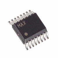
MAX1700EEE Maxim Integrated Products, MAX1700EEE Datasheet

MAX1700EEE
Specifications of MAX1700EEE
Available stocks
Related parts for MAX1700EEE
MAX1700EEE Summary of contents
Page 1
... Input Range Up to 800mA Output Step-Up Output (adjustable from 2.5V to 5.5V) PWM/PFM Synchronous-Rectified Topology External Clock or Internal 300kHz Oscillator 3µA Logic-Controlled Shutdown Power-Good Output (MAX1701) Low-Battery Comparator (MAX1701) Uncommitted Gain Block (MAX1701) PART MAX1700EEE MAX1701EEE Applications 16 I.C. 15 POUT PWM 14 OUT ...
Page 2
... CLK/SEL = GND P-Channel Turn-Off Current CLK/SEL = GND 2 _______________________________________________________________________________________ Operating Temperature Ranges MAX1700EEE, MAX1701EEE ...........................-40°C to +85°C +0.3V Junction Temperature ......................................................+150°C POUT Storage Temperature Range .............................-65°C to +160°C Lead Temperature (soldering, 10sec) .............................+300°C = 3.6V (Note 6); MAX1701: AIN = LBN = GND, LBP = REF, OUT = +25° ...
Page 3
Low-Noise, Step-Up DC-DC Converters ELECTRICAL CHARACTERISTICS (continued) (CLK/SEL = ONA = ONB = FB = PGND = GND, OUT = POUT 0°C to +85°C, unless otherwise noted. Typical values are PARAMETER GAIN BLOCK (MAX1701) ...
Page 4
High-Power (1A), Low-Noise, Step-Up DC-DC Converters ELECTRICAL CHARACTERISTICS (continued) (CLK/SEL = ONA = ONB = FB = PGND = GND, OUT = POUT -40°C to +85°C, unless otherwise noted.) (Note 8) A PARAMETER DC-DC ...
Page 5
Low-Noise, Step-Up DC-DC Converters ELECTRICAL CHARACTERISTICS (continued) (CLK/SEL = ONA = ONB = FB = PGND = GND, OUT = POUT -40°C to +85°C, unless otherwise noted.) (Note 8) A PARAMETER LOGIC AND CONTROL INPUTS 1.2V < ...
Page 6
High-Power (1A), Low-Noise, Step-Up DC-DC Converters (T = +25°C, unless otherwise noted.) A REFERENCE VOLTAGE vs. TEMPERATURE 1.254 1.252 1.250 1.248 1.246 1.244 -40 - 100 TEMPERATURE (°C) START-UP INPUT VOLTAGE vs. ...
Page 7
Low-Noise, Step-Up DC-DC Converters (Circuit of Figure +25°C, unless otherwise noted.) A LOAD-TRANSIENT RESPONSE A B 2ms/div V = 1.1V 3.3V IN OUT A = LOAD CURRENT, 0mA TO 200mA, 0.2A/div RIPPLE, ...
Page 8
High-Power (1A), Low-Noise, Step-Up DC-DC Converters PIN NAME MAX1700 MAX1701 — 1 LBP — 2 LBN 3 3 REF 4 4 CLK/SEL 5 5 GND — 6 POK ONB ONA — ...
Page 9
Low-Noise, Step-Up DC-DC Converters OUT IC PWR 2.25V ONA ON ONB 1.25V REF REF GND CLK/SEL FEEDBACK AND FB POWER-GOOD AIN* LBP* LBN* *MAX1701 ONLY Figure 1. Functional Diagram _______________Detailed Description The MAX1700/MAX1701 are highly efficient, low-noise power supplies for ...
Page 10
High-Power (1A), Low-Noise, Step-Up DC-DC Converters 0. MBR0520L MAX1700 LX OUT D1 MAX1701 CLK/SEL POUT 10 ONA OUT ONB 0.22 F REF FB FIXED GND PGND 0.22 F OUTPUT (GND) ...
Page 11
Low-Noise, Step-Up DC-DC Converters LOGIC HIGH ERROR COMPARATOR REF R 400mA CURRENT LIMIT Figure 4. Controller Block Diagram in Low-Power PFM Mode Synchronized PWM Operation By applying an external clock to CLK/SEL, the ...
Page 12
High-Power (1A), Low-Noise, Step-Up DC-DC Converters 0. MAX1701 LX POUT CLK/SEL 10 ONA ONB OUT 0. LBP POK VOLTAGE MONITOR LBO LOW-BATTERY MONITOR LBN R4 REF AO ARBITRARY VOLTAGE MONITOR AIN ...
Page 13
Low-Noise, Step-Up DC-DC Converters The MAX1700/MAX1701 have an internal 1.250V, 1% bandgap reference. Connect a 0.22µF bypass capaci- tor to GND within 0.2in. (5mm) of the REF pin. REF can source up to 50µA of external load current. Power-OK (MAX1701) ...
Page 14
High-Power (1A), Low-Noise, Step-Up DC-DC Converters 270k MAX1701 OUT ONB ON/OFF ONA 0.1 F 270k Figure 10. Momentary Pushbutton On/Off Switch Use a Schottky diode, such as a 1N5817, MBR0520L, or equivalent. The Schottky diode carries current ...
Page 15
Low-Noise, Step-Up DC-DC Converters low-noise power for DSP, control, and RF circuitry. Typically, RF phones spend most of their life in standby mode with only short periods in transmit/receive mode. During standby, maximize battery life by setting CLK/SEL = 0; ...
Page 16
High-Power (1A), Low-Noise, Step-Up DC-DC Converters Chip Information TRANSISTOR COUNT: 531 SUBSTRATE CONNECTED TO GND ________________________________________________________Package Information 16 ______________________________________________________________________________________ ...


