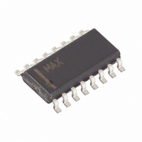
MAX797CSE Maxim Integrated Products, MAX797CSE Datasheet - Page 15

MAX797CSE
Manufacturer Part Number
MAX797CSE
Description
IC CONTRLR STEP-DOWN PWM 16-SOIC
Manufacturer
Maxim Integrated Products
Type
Step-Down (Buck)r
Datasheet
1.MAX797CSE.pdf
(32 pages)
Specifications of MAX797CSE
Internal Switch(s)
No
Synchronous Rectifier
Yes
Number Of Outputs
2
Voltage - Output
3.3V, 5V, Adj
Current - Output
10A
Frequency - Switching
150kHz, 300kHz
Voltage - Input
4.5 ~ 30 V
Operating Temperature
0°C ~ 70°C
Mounting Type
Surface Mount
Package / Case
16-SOIC (3.9mm Width)
Power - Output
696mW
Output Voltage
5 V
Output Current
10 A
Switching Frequency
340 KHz
Maximum Operating Temperature
+ 70 C
Mounting Style
SMD/SMT
Minimum Operating Temperature
0 C
Supply Current
0.44 mA
Case
sop
Dc
99+
Lead Free Status / RoHS Status
Contains lead / RoHS non-compliant
Available stocks
Company
Part Number
Manufacturer
Quantity
Price
Company:
Part Number:
MAX797CSE
Manufacturer:
MAXIM
Quantity:
9 800
Part Number:
MAX797CSE
Manufacturer:
MAXIM/美信
Quantity:
20 000
Company:
Part Number:
MAX797CSE+
Manufacturer:
Maxim
Quantity:
300
Company:
Part Number:
MAX797CSE+T
Manufacturer:
MAXIM
Quantity:
3
Company:
Part Number:
MAX797CSE-T
Manufacturer:
SP
Quantity:
226
Part Number:
MAX797CSE-T
Manufacturer:
MAXIM/美信
Quantity:
20 000
Figure 4. Main PWM Comparator Block Diagram
The output filter capacitor C2 sets a dominant pole in
the feedback loop. This pole must roll off the loop gain
to unity before the zero introduced by the output
capacitor’s parasitic resistance (ESR) is encountered
(see Design Procedure section). A 60kHz pole-zero
cancellation filter provides additional rolloff above the
unity-gain crossover. This internal 60kHz lowpass com-
pensation filter cancels the zero due to the filter capaci-
tor’s ESR. The 60kHz filter is included in the loop in
both fixed- and adjustable-output modes.
Synchronous rectification reduces conduction losses in
the rectifier by shunting the normal Schottky diode with
a low-resistance MOSFET switch. The synchronous rec-
tifier also ensures proper start-up of the boost-gate driv-
er circuit. If you must omit the synchronous power
MOSFET for cost or other reasons, replace it with a
small-signal MOSFET such as a 2N7002.
If the circuit is operating in continuous-conduction
mode, the DL drive waveform is simply the complement
of the DH high-side drive waveform (with controlled
dead time to prevent cross-conduction or “shoot-
through”). In discontinuous (light-load) mode, the syn-
chronous switch is turned off as the inductor current
falls through zero. The synchronous rectifier works
under all operating conditions, including idle mode.
The synchronous-switch timing is further controlled by
the secondary feedback (SECFB) signal in order to
improve multiple-output cross-regulation (see
Secondary Feedback-Regulation Loop section).
Synchronous-Rectifier Driver (DL Pin)
SLOPE COMPENSATION
CSH
CSL
REF
FB
______________________________________________________________________________________
I1
Synchronous Rectifier for CPU Power
R1
VL
I2
Step-Down Controllers with
R2
An internal regulator produces the 5V supply (VL) that
powers the PWM controller, logic, reference, and other
blocks within the MAX796. This +5V low-dropout linear
regulator can supply up to 5mA for external loads, with
a reserve of 20mA for gate-drive power. Bypass VL to
GND with 4.7µF. Important: VL must not be allowed to
exceed 6V. Measure VL with the main output fully
loaded. If VL is being pumped up above 5.5V, the
probable cause is either excessive boost-diode capaci-
tance or excessive ripple at V+. Use only small-signal
diodes for D2 (1N4148 preferred) and bypass V+ to
PGND with 0.1µF directly at the package pins.
The 2.505V reference (REF) is accurate to ±1.6% over
temperature, making REF useful as a precision system
reference. Bypass REF to GND with 0.33µF minimum.
REF can supply up to 1mA for external loads. However,
if tight-accuracy specs for either VOUT or REF are
essential, avoid loading REF with more than 100µA.
Loading REF reduces the main output voltage slightly,
according to the reference-voltage load regulation
error. In MAX799 applications, ensure that the SECFB
divider doesn’t load REF heavily.
When the main output voltage is above 4.5V, an internal P-
channel MOSFET switch connects CSL to VL while simul-
taneously shutting down the VL linear regulator. This
action bootstraps the IC, powering the internal circuitry
from the output voltage, rather than through a linear regu-
lator from the battery. Bootstrapping reduces power dissi-
pation caused by gate-charge and quiescent losses by
providing that power from a 90%-efficient switch-mode
source, rather than from a 50%-efficient linear regulator.
I3
UNCOMPENSATED
HIGH-SPEED
LEVEL TRANSLATOR
AND BUFFER
Internal VL and REF Supplies
OUTPUT DRIVER
TO PWM
LOGIC
15


