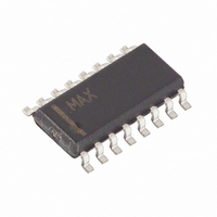
MAX1709ESE Maxim Integrated Products, MAX1709ESE Datasheet - Page 2

MAX1709ESE
Manufacturer Part Number
MAX1709ESE
Description
IC DC/DC CONV STEP-UP 4A 16-SOIC
Manufacturer
Maxim Integrated Products
Type
Step-Up (Boost)r
Datasheet
1.MAX1709ESE.pdf
(15 pages)
Specifications of MAX1709ESE
Internal Switch(s)
Yes
Synchronous Rectifier
No
Number Of Outputs
1
Voltage - Output
3.3V, 5V, Adj
Current - Output
4A
Frequency - Switching
600kHz
Voltage - Input
0.7 ~ 5 V
Operating Temperature
-40°C ~ 85°C
Mounting Type
Surface Mount
Package / Case
16-SOIC (3.9mm Width)
Power - Output
1.3W
Lead Free Status / RoHS Status
Contains lead / RoHS non-compliant
Other names
Q1226679
Available stocks
Company
Part Number
Manufacturer
Quantity
Price
Company:
Part Number:
MAX1709ESE
Manufacturer:
MAXIM
Quantity:
19
Company:
Part Number:
MAX1709ESE
Manufacturer:
MAXIM
Quantity:
106
Part Number:
MAX1709ESE+
Manufacturer:
MAXIM/美信
Quantity:
20 000
4A, Low-Noise, High-Frequency,
Step-Up DC-DC Converter
ABSOLUTE MAXIMUM RATINGS
ONA, ONB, OUT, SS/LIM, 3.3/5 to GND ...............-0.3V to +6.0V
LX to PGND ...........................................................-0.3V to +6.0V
FB, CLK, REF to GND.............................. -0.3V to (V
PGND to GND .......................................................-0.3V to +0.3V
Continuous Power Dissipation (T
ELECTRICAL CHARACTERISTICS
(V
Stresses beyond those listed under “Absolute Maximum Ratings” may cause permanent damage to the device. These are stress ratings only, and functional
operation of the device at these or any other conditions beyond those indicated in the operational sections of the specifications is not implied. Exposure to
absolute maximum rating conditions for extended periods may affect device reliability.
2
Output Voltage
Load Regulation
FB Regulation Voltage
FB Input Current
Output Voltage Adjust Range
Output Undervoltage Lockout
Frequency in Startup Mode
Minimum Startup Voltage
Minimum Operating Voltage
Soft-Start Pin Current
OUT Supply Current
OUT Leakage Current In
Shutdown
LX Leakage Current
n-Channel Switch
On-Resistance
n-Channel Current Limit
RMS Switch Current
Reference Voltage
Reference Load Regulation
Reference Supply Rejection
Input Low Level (Note 7)
OUT
16-Pin Narrow SO (derate 16.5mW/°C above +70°C) .....1.3W
28-Pin TSSOP Exposed Pad
(derate 23.8mW/°C above +70°C) ...................................1.9W
_______________________________________________________________________________________
= V
CLK
PARAMETER
= +3.6V, ONA = ONB = FB = GND, T
A
= +70°C)
V
Measured between 1A < I
I
V
(Note 3)
V
I
(Note 5)
V
V
V
V
SS/LIM = open
SS/LIM = 150kΩ to GND
MAX1709EUI+
MAX1709ESE
I
-1µA < I
+2.5V < V
ONA, ONB, 3.3/5, 1.2V < V
CLK, 2.7V < V
SW
OUT
REF
FB
FB
OUT
SS/LIM
FB
LX
ONB
= 1A
= +1.5V
= V
< 0.1V (Note 1)
= 1.5V (Note 6)
= 0
< 1mA (Note 1), T
=1.5V
= 3.6V
= 1V
ONB
REF
OUT
< 50µA
= V
OUT
A
OUT
< +5.5V
= 0°C to +85°C, unless otherwise noted. Typical values are at T
OUT
+ 0.3V)
< 5.5V
CONDITIONS
= +5.5V
A
= +25°C (Note 4)
SW
OUT
3.3/5 = GND, I
3.3/5 = OUT, I
< 3A (Note 2)
< 5.5V
Operating Temperature Range ...........................-40°C to +85°C
Junction Temperature ......................................................+150°C
Storage Temperature Range .............................-65°C to +150°C
Lead Temperature (soldering, 10s) .................................+300°C
28-Pin TSSOP Exposed Pad Junction-to-Exposed
Pad Thermal Resistance ......................................……1.2°C/W
SW
SW
= 1A
= 1A
1.215
1.245
3.26
4.92
MIN
2.5
2.0
3.2
7.5
3.5
40
1.240
1.260
-0.25
TYP
3.34
5.05
200
0.9
0.7
0.1
0.1
0.2
22
1
4
9
5
4
1.265
1.275
V
V
MAX
-0.45
0.2 ×
0.2 ×
3.42
5.17
A
200
400
440
5.5
2.3
1.1
5.0
6.5
OUT
OUT
40
40
12
10
10
5
6
5
= +25°C.)
UNITS
A
%/A
kHz
mΩ
mV
mV
nA
µA
µA
µA
µA
RMS
A
V
V
V
V
V
V
V
V


