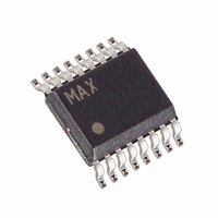
MAX1655EEE+T Maxim Integrated Products, MAX1655EEE+T Datasheet - Page 24

MAX1655EEE+T
Manufacturer Part Number
MAX1655EEE+T
Description
IC PWM STP-DN DC-DC CTRLR 16QSOP
Manufacturer
Maxim Integrated Products
Type
Step-Down (Buck)r
Datasheet
1.MAX1655ESE.pdf
(28 pages)
Specifications of MAX1655EEE+T
Internal Switch(s)
No
Synchronous Rectifier
Yes
Number Of Outputs
1
Voltage - Output
1 ~ 5.5 V
Current - Output
10A
Frequency - Switching
150kHz, 300kHz
Voltage - Input
4.5 ~ 30 V
Operating Temperature
-40°C ~ 85°C
Mounting Type
Surface Mount
Package / Case
16-QSOP
Power - Output
667mW
Output Voltage
1 V to 5.5 V
Output Current
10 A
Input Voltage
4.5 V to 30 V
Mounting Style
SMD/SMT
Maximum Operating Temperature
+ 85 C
Minimum Operating Temperature
- 40 C
Lead Free Status / RoHS Status
Lead free / RoHS Compliant
The major efficiency loss mechanisms under loads (in
the usual order of importance) are:
Inductor-core losses are fairly low at heavy loads
because the inductor’s AC current component is small.
Therefore, they aren’t accounted for in this analysis.
Ferrite cores are preferred, especially at 300kHz, but
powdered cores such as Kool-mu can work well.
where R
the MOSFET on-resistance, and R
sense resistor value. The R
cal MOSFETs for the high- and low-side switches
because they time-share the inductor current. If the
MOSFETs aren’t identical, their losses can be estimat-
ed by averaging the losses according to duty factor.
where VL is the MAX1652 internal logic supply voltage
(5V), and qG is the sum of the gate-charge values for
low- and high-side switches. For matched MOSFETs,
qG is twice the data sheet value of an individual
MOSFET. If V
this equation with V
improved by connecting VL to an efficient 5V source,
such as the system +5V supply.
where t
V
PD(tran) = transition loss =
where C
high-side MOSFET (a data sheet parameter), I
High-Efficiency, PWM, Step-Down
DC-DC Controllers in 16-Pin QSOP
24
__________Applications Information
FWD
Efficiency = P
______________________________________________________________________________________
V
of the IC
P(I
P(gate), gate-charge losses
P(diode), diode-conduction losses
P(tran), transition losses
P(cap), capacitor ESR losses
P(IC), losses due to the operating supply current
P
is the forward voltage of the Schottky.
BATT
Heavy-Load Efficiency Considerations
TOTAL
P(I
P(diode) = diode conduction losses
D
2
P(gate) = gate-driver loss = qG x f x VL
DC
RSS
R), I
is the diode conduction time (120ns typ) and
2
R) = (I
x I
is the DC resistance of the coil, R
is the reverse transfer capacitance of the
2
OUT
= P
= P(I
LOAD
R losses
P(cap) + P(IC)
= I
OUT
OUT
LOAD
is set to less than 4.5V, replace VL in
2
LOAD
BATT
R) + P(gate) + P(diode) + P(tran) +
x f x
/ P
/ (P
)
2
. In this case, efficiency can be
IN
x V
(
x (R
OUT
——————— + 20ns
x 100%
DS(ON)
V
FWD
BATT
DC
+ P
I
GATE
+ R
x t
TOTAL
x C
SENSE
term assumes identi-
D
DS(ON)
RSS
x f
) x 100%
is the current-
+ R
DS(ON)
SENSE
GATE
)
)
is
is
the DH gate-driver peak output current (1A typ), and
20ns is the rise/fall time of the DH driver.
where I
Input Capacitor Value section of the Design Procedure.
Under light loads, the PWM operates in discontinuous
mode, where the inductor current discharges to zero at
some point during the switching cycle. This causes the
AC component of the inductor current to be high com-
pared to the load current, which increases core losses
and I
light-load efficiency by using MOSFETs with moderate
gate-charge levels and by using ferrite, MPP, or other
low-loss core material. Avoid powdered iron cores; even
Kool-mu (aluminum alloy) is not as good as ferrite.
Good PC board layout is required to achieve specified
noise, efficiency, and stability performance. The PC
board layout artist must be provided with explicit
instructions, preferably a pencil sketch of the place-
ment of power switching components and high-current
routing. See the evaluation kit PC board layouts in the
MAX1653, MAX796, and MAX797 EV kit manuals for
examples. A ground plane is essential for optimum per-
formance. In most applications, the circuit will be locat-
ed on a multilayer board, and full use of the four or
more copper layers is recommended. Use the top layer
for high-current connections, the bottom layer for quiet
connections (REF, SS, GND), and the inner layers for
an uninterrupted ground plane. Use the following step-
by-step guide.
1) Place the high-power components (C1, C2, Q1, Q2,
__PC Board Layout Considerations
P(cap) = input capacitor ESR loss = (I
D1, L1, and R1) first, with their grounds adjacent.
Priority 1: Minimize current-sense resistor trace
Priority 2: Minimize ground trace lengths in the
Priority 3: Minimize other trace lengths in the high-
Ideally, surface-mount power components are
butted up to one another with their ground terminals
almost touching. These high-current grounds (C1-,
C2-, source of Q2, anode of D1, and PGND) are
then connected to each other with a wide filled zone
2
R losses in the output filter capacitors. Obtain best
RMS
Light-Load Efficiency Considerations
is the input ripple current as calculated in the
lengths (see Figure 9).
high-current paths (discussed below).
current paths. Use >5mm wide traces.
Q2: 5mm max length LX node (Q1
source, Q2 drain, D1 cathode, inductor):
15mm max length
C1 to Q1: 10mm max length. D1 anode to
RMS
)
2
x R
ESR


