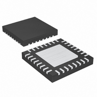
MAX5072ETJ+T Maxim Integrated Products, MAX5072ETJ+T Datasheet - Page 21

MAX5072ETJ+T
Manufacturer Part Number
MAX5072ETJ+T
Description
IC CONV BUCK/BOOST 32-TQFN
Manufacturer
Maxim Integrated Products
Type
Step-Down (Buck), Step-Up (Boost)r
Datasheet
1.MAX5072ETJ.pdf
(27 pages)
Specifications of MAX5072ETJ+T
Internal Switch(s)
Yes
Synchronous Rectifier
No
Number Of Outputs
2
Voltage - Output
0.8 ~ 28 V
Current - Output
1A, 2A
Frequency - Switching
200kHz ~ 2.2MHz
Voltage - Input
4.5 ~ 23 V
Operating Temperature
-40°C ~ 85°C
Mounting Type
Surface Mount
Package / Case
32-TQFN Exposed Pad
Power - Output
2.76W
Lead Free Status / RoHS Status
Lead free / RoHS Compliant
For the boost converter:
where V
the Electrical Characteristics for the R
where t
MOSFET. The t
measured in the actual application.
The supply current in the MAX5072 is dependent on
the switching frequency. See the Typical Operating
Characteristics to find the supply current of the
MAX5072 at a given operating frequency. The power
dissipation (P
is calculated using following equation.
The total power dissipation P
R
I
P
DS
RMS
T
and t
= P
P
P
is the drop across the internal MOSFET. See
SW
SW
Converter with POR and Power-Fail Output
=
S
DC1
) in the device due to supply current (I
P
R
F
=
=
(
P
DC
I
2
S
are rise and fall times of the internal
and t
∆I
V
V
DC
______________________________________________________________________________________
INMAX
+ P
=
O
L
=
V
I
IN
+I
=
I
I
I
×
DC
PK
2
INMAX
DC2
F
RMS
(
I
2
=
IN
V
PK
are typically 20ns, and can be
IN
=
=
V
V
×
IN
I
×
+ P
O
L
IN
I
+(I
−
IN
×
I
O
(
T
×
×
×
R
V
× η
t
−
+
R
4
DC
DS
SW1
DS(ON)MAX
in the device is:
I
I
2.2MHz, Dual-Output Buck or Boost
×
f
O
SUPPLY
SW
∆
4
∆
(
2
+
I
)
2
t
L
I
×
R
L
t
×
+ P
I
F
PK
+
D
)
DS(ON)MAX
×
))
SW2
t
F
f
×
)
SW
×
D
+ P
MAX
f
3
SW
S
value.
S
)
where P
converter 2, respectively. P
losses in converter 1 and converter 2, respectively.
Calculate the temperature rise of the die using the fol-
lowing equation:
where θ
of the package equal to +2°C/W. Solder the exposed
pad of the package to a large copper area to minimize
the case-to-ambient thermal impedance. Measure the
temperature of the copper area near the device at a
worst-case condition of power dissipation and use
+2°C/W as θ
ent thermal impedance (θ
well the heat is transferred from the PC board to the
ambient. Use large copper area to keep the PC board
temperature low. The θ
+40°C/W range.
The MAX5072 provides an internal transconductance
amplifier with its inverting input and its output available
to the user for external frequency compensation. The
flexibility of external compensation for each converter
offers wide selection of output filtering components,
especially the output capacitor. For cost-sensitive
applications, use high-ESR aluminum electrolytic
capacitors; for component size-sensitive applications,
use low-ESR tantalum or ceramic capacitors at the out-
put. The high switching frequency of MAX5072 allows
use of ceramic capacitors at the output.
Choose all the passive power components that meet
the output ripple, component size, and component cost
requirements. Choose the small-signal components for
the error amplifier to achieve the desired closed-loop
bandwidth and phase margin. Use a simple pole-zero
pair (Type II) compensation if the output capacitor ESR
zero frequency is below the unity-gain crossover fre-
quency (f
the ESR zero frequency is higher than f
pensating for a continuous mode boost converter that
has a right-half plane zero.
Use the following procedure 1 to calculate the compen-
sation network components when f
Procedure 1 (see Figure 7):
Calculate the f
DC1
J-C
C
). Type III compensation is necessary when
is the junction-to-case thermal impedance
and P
J-C
ZERO,ESR
thermal impedance. The case-to-ambi-
T
DC2
J
= T
Buck Converter Compensation
are DC losses in converter 1 and
C-A
C
and LC double pole:
+ (P
SW1
is usually in the +20°C/W to
C-A
T
) is dependent on how
x θ
and P
J-C
ZERO,ESR
Compensation
)
SW2
C
or when com-
are switching
< f
C
.
21


