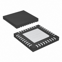
MAX15015AATX+ Maxim Integrated Products, MAX15015AATX+ Datasheet - Page 14

MAX15015AATX+
Manufacturer Part Number
MAX15015AATX+
Description
IC DC/DC CONV 1A 36-TQFN-EP
Manufacturer
Maxim Integrated Products
Type
Step-Down (Buck)r
Datasheet
1.MAX15017AATX.pdf
(26 pages)
Specifications of MAX15015AATX+
Internal Switch(s)
Yes
Synchronous Rectifier
Yes
Number Of Outputs
2
Voltage - Output
1.26 ~ 32 V
Current - Output
1A
Frequency - Switching
135kHz ~ 500kHz
Voltage - Input
4.5 ~ 40 V
Operating Temperature
-40°C ~ 125°C
Mounting Type
Surface Mount
Package / Case
36-TQFN Exposed Pad
Power - Output
2.1W
Lead Free Status / RoHS Status
Lead free / RoHS Compliant
1A, 4.5V to 40V Input Buck Converters with
50mA Auxiliary LDO Regulators
The MAX15014–MAX15017 combine a voltage-mode
buck converter with an internal 0.5Ω power MOSFET
switch and a low-quiescent-current LDO regulator. The
buck converter of the MAX15015/MAX15016 has a
wide input voltage range of 4.5V to 40V. The
MAX15014/MAX15017’s input voltage range is 7.5V to
40V. Fixed switching frequencies of 135kHz and
500kHz are available. The internal low R
allows for up to 1A of output current, and the output
voltage can be adjusted from 1.26V to 32V. External
compensation and voltage feed-forward simplify loop
compensation design and allow for a wide variety of L
and C filter components. All devices offer an automatic
switchover to pulse-skipping (PFM) mode, providing
low quiescent current and high efficiency at light loads.
Under no load, PFM mode operation reduces the cur-
rent consumption to 5.6mA for the MAX15014/
MAX15017 and 8.6mA for the MAX15015/MAX15016. In
shutdown (DC-DC and LDO regulator off), the supply
Figure 1. MAX15015/MAX15016 Simplified Block Diagram
14
EN_SW
COMP
SYNC
SGND
REG
SS
FB
______________________________________________________________________________________
I
SS
REG_LDO
IN_SW
OSC
EN
VREG_OK
V
REF
INT
IN_LDO
IN S/W
RAMP
Detailed Description
V
V
V
+
-
REF
REFOK
E/A
REF
-
-
+
+
-
V
VINT
0.3V
INT
THERMAL
7.0V OR 4.1V
V
SHDN
INT
UVLO_SW
V
CLK
V
+
V
REFOK
INTOK
V
REFOK
INTOK
4.1V
SHDN
CPWM
TSD
+
-
TSD
DS_ON
UVLO_SW
SSA
UVLO_LDO
+
-
V
REG_EN
UVLO_LDO
VREG_ OK
V
SHDN
REF
V
INTOK
TSD
V
INT
switch
EN_SYS
PREREG
SHDN
0.925 x V
EN
IN_LDO
REF
OVERL
current falls to 6µA. Additional features include a pro-
grammable soft-start, cycle-by-cycle current limit,
hiccup-mode output short-circuit protection, and thermal
shutdown.
The LDO linear regulator operates from 5V to 40V and
delivers a guaranteed 50mA load current. The devices
feature a preset output voltage of 5.0V (MAX1501_A) or
3.3V (MAX1501_B). Alternatively, the output voltage
can be adjusted from 1.5V to 11V using an external
resistive divider. The LDO section also features a
RESET output with adjustable timeout period.
The MAX15014–MAX15017 feature two logic inputs,
EN_SW (active-high) and EN_SYS (active-high) that can
be used to enable the switching power supply and the
LDO_OUT outputs. When V
threshold and EN_SYS is high, the switching power sup-
ply is enabled. When EN_SYS is high, the LDO is active.
When EN_SYS is low, the entire chip is off (see Table 1).
ENABLE LDO
-
+
MANAGEMENT
V
OVERLOAD
PFM
INT
2µA
PASS ELEMENT
MAX15015/MAX15016
CLK
+
-
V
LOGIC
INT
PFM
DELAY COMPARATOR
V
REF_ILIM
REF
V
-
+
INT
SCLK
PCLK
+
-
+
-
OUT_LDO
V
REF
REF_PFM
DVREG
PCLK
Enable Inputs and UVLO
MUX
HIGH-SIDE
CURRENT
EN_SW
SENSE
DVREG
V
INT
C-
is higher than the
185mV
LEVEL
SHIFT
C+
DVREG
LDO_OUT
SET_LOD
RESET
CT
DRAIN
BST
LX
PGND


