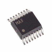
MAX686EEE+ Maxim Integrated Products, MAX686EEE+ Datasheet - Page 2

MAX686EEE+
Manufacturer Part Number
MAX686EEE+
Description
IC SUPPLY LCD BIAS INV 16-QSOP
Manufacturer
Maxim Integrated Products
Type
Step-Up (Boost), Invertingr
Datasheet
1.MAX686EEE.pdf
(16 pages)
Specifications of MAX686EEE+
Internal Switch(s)
Yes
Synchronous Rectifier
No
Number Of Outputs
1
Voltage - Output
±27.5V
Current - Output
100mA
Frequency - Switching
300kHz
Voltage - Input
2.7 ~ 5.5 V
Operating Temperature
-40°C ~ 85°C
Mounting Type
Surface Mount
Package / Case
16-QSOP
Power - Output
667mW
Lead Free Status / RoHS Status
Lead free / RoHS Compliant
ABSOLUTE MAXIMUM RATINGS
Voltage
Current
DAC-Controlled Boost/Inverter
LCD Bias Supply with Internal Switch
Stresses beyond those listed under “Absolute Maximum Ratings” may cause permanent damage to the device. These are stress ratings only, and functional
operation of the device at these or any other conditions beyond those indicated in the operational sections of the specifications is not implied. Exposure to
absolute maximum rating conditions for extended periods may affect device reliability.
ELECTRICAL CHARACTERISTICS
(V
2
V
FB, REF, DACOUT to GND.......................-0.3V to (V
PGND to GND .....................................................-0.3V to +0.3V
LX, LCDON to GND..............................................-0.3V to +30V
LX (sinking) .....................................................................600mA
LCDON (sinking)...............................................................10mA
LX
Supply Voltage (Note 1)
Input Voltage
Supply Current
Shutdown Current
V
V
Hysteresis
V
Line Regulation
Load Regulation
LX Voltage Range
LX Switch Current Limit
LX On-Resistance
LX Leakage Current
Maximum LX On-Time
Minimum LX Off-Time
CC
CC
CC
CC
CC
UP, DN, V
_______________________________________________________________________________________
, ISET, POK, POL, SHDN,
= V
Undervoltage Lockout
Undervoltage Lockout
DAC Reset Threshold
DD
PARAMETER
= V
DD
IN
to GND ...........................................-0.3V to +6V
= +5V, C
REF
= 0.1µF, T
SYMBOL
V
I
CC
I
V
CC
V
LXLEAK
I
SHDN
RESET
t
LOCK
V
R
V
t
OFF
I
ON
LX
+ I
, V
LX
LX
IN
A
DD
DD
= 0°C to +85°C, unless otherwise noted. Typical values are at T
Voltage applied to L1
POL = GND, V
SHDN = GND
Rising or falling
Boost configuration, V
I
Boost configuration, V
I
ISET = V
ISET = GND
V
V
V
POL = GND, V
POL = V
POL = GND, V
POL = V
LOAD
LOAD
CC
CC
LX
CC
= 28V
= V
= V
+ 0.3V)
= 5mA, V
= 0mA to 5mA
DD
DD
CC
CC
CC
, V
, V
= 5V, I
= 3.3V, I
FB
FB
FB
FB
FB
CONDITIONS
CC
< 0.15V
> 0.4V
= 1.3V, I
> 1.2V
< 0.8V
LX
= V
Continuous Power Dissipation (T
Operating Temperature Ranges
Storage Temperature Range .............................-65°C to +160°C
Lead Temperature (soldering, 10sec) .............................+300°C
LX
QSOP (derate 8.30mW/°C above +70°C) ......................667mW
MAX686C/D ..........................................................0°C to +70°C
MAX686EEE.......................................................-40°C to +85°C
= 100mA
OUT
OUT
DD
= 100mA
= 2.7V to 5.5V
DACOUT
= 27.5V,
= 27.5V,
= 0mA
2.10
0.42
0.21
MIN
2.7
0.8
0.5
0.8
2.8
8
4
4
A
= +70°C)
A
TYP
0.01
0.50
0.25
100
1.3
2.5
1.5
0.1
0.6
0.8
3.5
65
10
1
5
5
= +25°C.)
V
MAX
2.65
0.58
0.29
125
5.5
2.1
1.2
1.6
1.5
1.2
4.2
OUT
28
12
4
6
6
UNITS
%/mA
%/V
mV
µA
µA
µA
µs
µs
V
V
V
V
V
A


