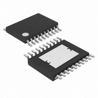
MAX5096AAUP+ Maxim Integrated Products, MAX5096AAUP+ Datasheet - Page 12

MAX5096AAUP+
Manufacturer Part Number
MAX5096AAUP+
Description
IC DC-DC CONV BUCK 20TSSOP
Manufacturer
Maxim Integrated Products
Type
Step-Down (Buck)r
Datasheet
1.MAX5097AATE.pdf
(21 pages)
Specifications of MAX5096AAUP+
Internal Switch(s)
Yes
Synchronous Rectifier
No
Number Of Outputs
2
Voltage - Output
3.3V, 1.24 ~ 11 V
Current - Output
600mA
Frequency - Switching
135kHz
Voltage - Input
5 ~ 40 V
Operating Temperature
-40°C ~ 125°C
Mounting Type
Surface Mount
Package / Case
20-TSSOP Exposed Pad, 20-eTSSOP, 20-HTSSOP
Power - Output
1.74W
Lead Free Status / RoHS Status
Lead free / RoHS Compliant
The output voltages of multiple MAX5096/MAX5097
converters can be made to track by using the SS pin
during turn-on and turn-off (see Figure 3). SS is pulled
up using a 5µA current source and connecting SS of
multiple MAX5096/MAX5097s, raising the references
with the same slope. Tracking the converters reduces
the differential voltages between the core and I/O volt-
ages during turn-on, turn-off, and brownout. If any one
converter output drops due to shutdown or an overload
fault situation, the SS drops, pulling down all the con-
verters simultaneously. The rate of fall of output volt-
ages, however, depends on the output capacitance
and load of the individual converter.
Multiple voltage sequencing can be done by daisy-
chaining several MAX5096/MAX5097s. The RESET of
the first converter can be connected to EN of the sec-
ond converter. This allows the first converter to come
up first every time the system is powered up.
A supervisor circuit is integrated in the MAX5096/
MAX5097. RESET is an open-drain output. RESET pulls
low as soon as V
regulation voltage. Once the output voltage rises above
92% of the set output voltage, the RESET output enters
40V, 600mA Buck Converters with Low-
Quiescent-Current Linear Regulator Mode
Figure 2. Fixed Output Voltage Configuration
12
______________________________________________________________________________________
Output Voltage Tracking/Sequencing
Power-On Reset Output (
OUT
0.047μF
drops below 90% of its nominal
22pF
C
C
SS
V
P
IN
100μF
C
IN
100kΩ
1.2nF
0.01μF
C
R
C
C
C
CT
SS
V
EN
SYNC
COMP
CT
LDO/BUCK
IN
RESET )
GND
MAX5096
MAX5097
PGND
a high-impedance state after the active timeout period
(t
mable using a single capacitor from CT to ground. Use
the following equation to calculate the required timeout
period for the power-on reset:
where V
and C
To obtain a logic-voltage output, connect a pullup
resistor from RESET to a logic-supply voltage. The
internal open-drain MOSFET can sink 1mA while provid-
ing a TTL logic-low signal. If unused, ground RESET or
leave it unconnected.
The power-on reset behavior is the same in both the
LDO and Buck Modes of operation.
The MAX5096/MAX5097 internal oscillator generates a
factory-preset frequency of either 135kHz (MAX5096)
or 330kHz (MAX5097). The 135kHz version keeps the
maximum fundamental frequency below 150kHz, which
keeps the third harmonic below 450kHz and under the
RP
RESET
). The active timeout period is externally program-
Oscillator/Synchronization Input (SYNC)
OUT
ADJ
LX
BP
CT
CT-TH
is in Farads.
*USE MURS105 IN APPLICATIONS
D1*
B260/
MURS105
WHERE LDO MODE QUIESCENT
CURRENT IS CRITICAL.
is 1.237V, I
1.0μF
22μH
t
RP
(CER.)
22μF
C
OUT
=
V
100kΩ
CT TH
I
CH
CH
+
−
is 1µA, t
×
C
V
CT
RESET
OUT
RP
is in seconds,


