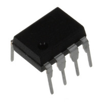
NJM2352D NJR, NJM2352D Datasheet

NJM2352D
Specifications of NJM2352D
Available stocks
Related parts for NJM2352D
NJM2352D Summary of contents
Page 1
... FEATURES • Operating Voltage (2.6V to 24.0V) • Low Operating Current • Internal Low Voltage Detect Circuit • Pulse Width Modulation Control Circuit • Package Outline DIP8, DMP8 • Bipolar Technology ■ BLOCK DIAGRAM Ver.2003-07-18 ■ PACKAGE OUTLINE NJM2352D NJM2352D NJM2352M NJM2352M - 1 - ...
Page 2
ABSOLUTE MAXIMUM RATINGS PARAMETER SYMBOL Supply Voltage Power Dissipation P Operating Temperature Range T Storage Temperature Range T ■ ELECTRICAL CHARACTERISTICS DC Electrical Characteristics ( 25ºC) PARAMETER Operating Current (1) Operating Current (2) Reference Voltage ...
Page 3
TYPICAL APPLICATION 1. Step-Up Switching Regulator (Low Current) 2. Step-Up Switching Regulator (High Current) Ver.2003-07- ...
Page 4
TYPICAL APPLICATION 3. Step-Down Switching Regulator 4. Inverting Switching Regulator - 4 - Ver.2003-07-18 ...
Page 5
DESIGN EQUSTIONS Component (pF 100µ low battery detection voltage. TH Ripple Voltage ...
Page 6
DESCRIPTION The NJM2352 is a micro-power switching regulator control IC suitable for a equipment of battery operation and may be used as step-up, step-down and inverting regulators. The NJM2352 contains a reference, oscillator, amplifier, comparator, detector of input voltage ...
Page 7
TERMINAL DESCRIPTION TERMINAL NO. TERMINAL ITEMS 2 Timing C 3 Switching Transistor Output 4 GROUND + 5 V Ver.2003-07-18 FUNCTION Connecting timing for deciding oscillator frequency. Open collector Output of switching transistor. Ground Supply voltage terminal. INSIDE EQUIVALENT CIRCUITS ...
Page 8
TERMINAL DESCRIPTION TERMINAL NO. TERMINAL ITEMS 6 NF2 7 NF1 - 8 - FUNCTION Terminal from connecting point of AMP output and COMP-1 inverting input. Inverting input of amplifier. INSIDE EQUIVALENT CIRCUITS Ver.2003-07-18 ...
Page 9
PRINCIPLE OF OPERATION The NJM2352 circuit block is shown on Fig. 1 and timing chart on Fig. 2. Function of COMP-2 is setting dead-time. At point A is the square wave and at point B is the triangular wave. ...
Page 10
MINIMUM OPERATING VOLTAGE Minimum operating voltage is V design. Less than this minimum operating voltage, internal switching transistor becomes on, and the surge-like high current flows into it especially in Step-Up or Inverting application. ■ OSCILLATOR Oscillator frequency is ...
Page 11
EFFICIENCY Efficiency is shown below. V − Set OUT − Step Down = − Inverting = x ...
Page 12
TYPICAL CHARACTERISTICS Reference Voltage Operating Frequency Switching Tr Saturation Voltage - 12 - Operating Current Operating Frequency V (No. 8 Pin) CE Ver.2003-07-18 ...
Page 13
TYPICAL CHARACTERISTICS Minimum Operating Input Voltage No.1 Pin Input Current Ver.2003-07-18 Voltage Gain - 13 - ...
Page 14
TYPICAL CHARACTERISTICS Output Voltage Output Voltage - 14 - (APPLICATION) Efficiency Output Voltage Ver.2003-07-18 ...
Page 15
TYPICAL CHARACTERISTICS (Test Circuits 2) Efficiency Efficiency Input Current Ver.2003-07-18 Output Voltage Output Voltage Output Voltage - 15 - ...
Page 16
The specifications on this databook are only given for information , without any guarantee as regards either mistakes or omissions. The application circuits in this databook are described only to show representative usages of the product ...


