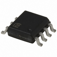
MIC4680-5.0BM Micrel Inc, MIC4680-5.0BM Datasheet - Page 12

MIC4680-5.0BM
Manufacturer Part Number
MIC4680-5.0BM
Description
IC REG BUCK 1A 5.0V 8SOIC
Manufacturer
Micrel Inc
Series
SuperSwitcher™r
Type
Step-Down (Buck)r
Datasheet
1.MIC4680-5.0YM_TR.pdf
(15 pages)
Specifications of MIC4680-5.0BM
Internal Switch(s)
Yes
Synchronous Rectifier
No
Number Of Outputs
1
Voltage - Output
5V
Current - Output
1A
Frequency - Switching
200kHz
Voltage - Input
4 ~ 34 V
Operating Temperature
-40°C ~ 125°C
Mounting Type
Surface Mount
Package / Case
8-SOIC (3.9mm Width)
Input Voltage
12V
Output Current
1.3A
Output Voltage
5V
No. Of Outputs
1
Supply Voltage Range
4V To 34V
No. Of Pins
8
Operating Temperature Range
-40°C To +125°C
Peak Reflow Compatible (260 C)
No
Lead Free Status / RoHS Status
Contains lead / RoHS non-compliant
Power - Output
-
Lead Free Status / RoHS Status
Contains lead / RoHS non-compliant, Contains lead / RoHS non-compliant
Available stocks
Company
Part Number
Manufacturer
Quantity
Price
Company:
Part Number:
MIC4680-5.0BM
Manufacturer:
MIC
Quantity:
1
Calculate the worst-case junction temperature:
where:
Calculating the maximum junction temperature given a
maximum ambient temperature of 65°C:
This value is less than the allowable maximum operating
junction temperature of 125°C as listed in “Operating
Ratings.” Typical thermal shutdown is 160°C and is
listed in “Electrical Characteristics.”
Increasing the Maximum Output Current
The maximum output current at high input voltages can
be increased for a given board layout. The additional
three components shown in Figure 4 will reduce the
overall loss in the MIC4680 by about 20% at high V
and high I
Even higher output current can be achieved by using the
MIC4680 to switch an external FET. See Figure 9 for a
5A supply with current limiting.
Micrel, Inc.
March 2008
T
T
P
θ
T
T
T
TJ = 1.064 × 20°C/W + (45°C – 25°C) + 65°C
TJ = 106.3°C
P
P
P
JC
J
J
C
A
A(max)
D(IC)
D
D
D
OUT
= P
= MIC4680 junction temperature
= ambient temperature at which T
= “pin” temperature measurement taken at
= junction-to-case thermal resistance.
4V to +34V
=
=
=
.
1.33W
= MIC4680 power dissipation
GND
P
0.79
The θ
is approximately 20°C/W. (Also see Figure
1.)
the entry point of pins 6 or 7 into the
plastic
temperature (T
measured.
the specific design.
D(IC)
5W
V
J1
J3
= maximum ambient operating temp. for
OUT
IN
η
15µF
35V
C1
θ
* C3 can be used to provide additional stability
JC
and improved transient response.
−
−
JC
5W
+ (T
P
OUT
for the MIC4680’s power-SOIC-8
OFF
ON
package
C
S1
NKK G12AP
– T
A
) at which T
0.1µF
A
) + T
50V
C2
A(max)
at
Figure 6a. Evaluation Board Schematic Diagram
2
1
SOIC-8
IN
SHDN
U1 MIC4680BM
C
the
is measured.
GND
C
5–8
is
ambient
SW
FB
3
4
IN
D1
B260A
or
SS26
12
68µH
L1
R6
optional
Layout Considerations
Layout is very important when designing any switching
regulator. Rapidly changing switching currents through
the printed circuit board traces and stray inductance can
generate voltage transients which can cause problems.
To minimize stray inductance and ground loops, keep
trace lengths, indicated by the heavy lines in Figure 5, as
short as possible. For example, keep D1 close to pin 3
and pins 5 through 8, keep L1 away from sensitive node
FB, and keep C
“Applications Information: Thermal Considerations” for
ground plane layout.
The feedback pin should be kept as far way from the
switching elements (usually L1 and D1) as possible.
A circuit with sample layouts is provided. See Figure 6a
through 6e.
+4V to +34V
Power
SOIC-8
V
1
2
IN
Figure 4. Increasing Maximum Output Current
R1
3.01k
R2
6.49k
JP1a
1.8V
C
IN
IN
SHDN
3
4
MIC4680BM
Figure 5. Critical Traces for Layout
R3
2.94k
2
1
JP1b
2.5V
C3*
optional
5 6 7 8
GND
IN
SHDN
IN
MIC4680BM
5
6
close to pin 2 and pins 5 though 8. See
at High Input Voltages
5 6 7 8
GND
R4
1.78k
JP1c
3.3V
SW
FB
7
8
SW
FB
3
R5
JP1d
5.0V
3
4
1N4148
2.2nF
D1
C4
220µF
10V
68µH
L1
V
C5
0.1µF
50V
GND
M9999-032808
1A
J2
OUT
J4
C
OUT
D1
MIC4680
R1
R2
GND
V
OUT


