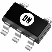
NCP1450ASN30T1G ON Semiconductor, NCP1450ASN30T1G Datasheet - Page 21

NCP1450ASN30T1G
Manufacturer Part Number
NCP1450ASN30T1G
Description
IC CTRLR DC-DC PWM 3.0V SOT23-5
Manufacturer
ON Semiconductor
Type
Step-Up (Boost), Inverting, Flyback, Forward Converter, Sepicr
Datasheet
1.NCP1450ASN19T1.pdf
(22 pages)
Specifications of NCP1450ASN30T1G
Internal Switch(s)
No
Synchronous Rectifier
No
Number Of Outputs
1
Voltage - Output
3V
Current - Output
1A
Frequency - Switching
180kHz
Voltage - Input
0.6 ~ 5.5 V
Operating Temperature
-40°C ~ 85°C
Mounting Type
Surface Mount
Package / Case
TSOT-23-5, TSOT-5, TSOP-5
Power - Output
500mW
Mounting Style
SMD/SMT
Lead Free Status / RoHS Status
Lead free / RoHS Compliant
Other names
NCP1450ASN30T1GOS
NCP1450ASN30T1GOS
NCP1450ASN30T1GOSTR
NCP1450ASN30T1GOS
NCP1450ASN30T1GOSTR
Available stocks
Company
Part Number
Manufacturer
Quantity
Price
Company:
Part Number:
NCP1450ASN30T1G
Manufacturer:
ON Semiconductor
Quantity:
5 100
Part Number:
NCP1450ASN30T1G
Manufacturer:
ON/安森美
Quantity:
20 000
PCB Layout Hints
Grounding
return ground, the input power return ground, and the device
switch ground to reduce noise. In Figure 73, e.g.: C2 GND,
C1 GND, and IC1 GND are connected at one point in the
evaluation board. The input ground and output ground traces
must be thick enough for current to flow through and for
reducing ground bounce.
Power Signal Traces
power carrying traces to reduce power loss so as to improve
efficiency (short and thick traces for connecting the inductor
L can also reduce stray inductance), e.g.: short and thick
traces listed below are used in the evaluation board:
One point grounding should be used for the output power
Low resistance conducting paths should be used for the
1. Trace from TP1 to L1
2. Trace from L1 to anode pin of D1
3. Trace from cathode pin of D1 to TP3
GND
GND
TP5
TP6
V
TP2
TP1
V
IN
IN
10 mF
10 mF
C5
C2
Figure 73. NCP1450A Evaluation Board Schematic Diagram 1 (Step−up
Figure 74. NCP1450A Evaluation Board Schematic Diagram 2 (Step−up
OFF
DC−DC Converter Using External Bipolar Transistor Switch)
ON
OFF
CE
ON
CE
JP2
DC−DC Converter Using External MOSFET Switch)
JP1
C6
0.1 mF
C3
0.1 mF
OUT
NC
CE
1
2
3
OUT
NC
http://onsemi.com
CE
2
3
1
10 mH
NCP1450A
L2
10 mH
L1
21
GND
EXT
5
4
Output Capacitor
terminals to obtain better smoothing effect on the output
ripple.
Switching Noise Decoupling Capacitor
OUT pin and GND pin of the NCP1450A to filter the
switching spikes in the output voltage monitored by the
OUT pin.
IC2
The output capacitor should be placed close to the output
A 0.1 mF ceramic capacitor should be placed close to the
GND
EXT
5
4
NTGS3446T1
IC1
3000 pF
560
Rb
Cb
Q1
MBRM110L
Q2
MMJT9410
MBRM110L
D1
D2
C1
220 mF
C4
220 mF
TP3
V
TP4
GND
OUT
TP7
V
TP8
GND
OUT


