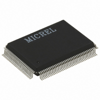
KSZ8995XA Micrel Inc, KSZ8995XA Datasheet - Page 13

KSZ8995XA
Manufacturer Part Number
KSZ8995XA
Description
IC SWITCH 10/100 5PORT 128PQFP
Manufacturer
Micrel Inc
Specifications of KSZ8995XA
Applications
*
Mounting Type
Surface Mount
Package / Case
128-MQFP, 128-PQFP
Number Of Primary Switch Ports
5
Internal Memory Buffer Size
64
Operating Supply Voltage (typ)
1.8/2.5/3.3V
Fiber Support
Yes
Integrated Led Drivers
Yes
Phy/transceiver Interface
MII/SNI
Power Supply Type
Analog/Digital
Package Type
PQFP
Data Rate (typ)
10/100Mbps
Vlan Support
Yes
Operating Temperature (max)
70C
Operating Temperature (min)
0C
Pin Count
128
Mounting
Surface Mount
Jtag Support
No
Operating Temperature Classification
Commercial
Lead Free Status / RoHS Status
Lead free / RoHS Compliant
For Use With
576-1642 - BOARD EVALUATION FOR KSZ8995XA
Lead Free Status / RoHS Status
Compliant, Lead free / RoHS Compliant
Other names
576-1042
Available stocks
Company
Part Number
Manufacturer
Quantity
Price
Company:
Part Number:
KSZ8995XA
Manufacturer:
MICREL
Quantity:
1 334
Company:
Part Number:
KSZ8995XA
Manufacturer:
MICREL30
Quantity:
348
Part Number:
KSZ8995XA
Manufacturer:
MICREL
Quantity:
20 000
September 2008
Notes:
1.
2.
Pin Number
106
107
108
109
110
111
112
113
114
115
116
117
118
119
120
121
122
123
124
125
126
127
128
P = Power supply.
I = Input.
O = Output.
I/O = Bidirectional.
Gnd = Ground.
Ipu = Input w/internal pull-up.
Ipd = Input w/internal pull-down.
Ipd/O = Input w/internal pull-down during reset, output pin otherwise.
Ipu/O = Input w/internal pull-up during reset, output pin otherwise.
NC = No connect.
PU = Strap pin pull-up.
PD = Strap pull-down.
Otri = Output tristated.
Pin Name
Reserved
Reserved
SCANEN
TESTEN
LED1-0
VDDAP
VDDAR
RST_N
TEST2
GNDD
GNDA
GNDA
GNDA
VDDC
MDIO
MDC
SDA
SCL
PS1
PS0
NC
X1
X2
Type
Ipu/O
Ipu/O
Gnd
Gnd
Gnd
Gnd
Ipu
Ipd
Ipd
Ipu
Ipd
Ipd
NC
I/O
I/O
O
P
P
P
I
(1)
Port
All
All
All
All
All
All
1
Pin Function
LED indicator 0.
Switch or PHY[5] MII management data clock.
Switch or PHY[5] MII management data I/O.
No connect.
Output clock at 81kHz in I
Serial data input/output in I
No connect
No connect or pull-down.
No connect or pull-down.
Reset the KS8995XA. Active low.
Digital ground.
1.8V digital core V
Factory test pin.
Factory test pin.
No connection.
25MHz crystal clock connection/or 3.3V tolerant oscillator input.
Oscillator should be ±100ppm.
25MHz crystal clock connection.
1.8V analog V
Analog ground.
1.8V analog V
Analog ground.
Analog ground.
Factory test pin.
13
DD
DD
(2)
.
for PLL.
DD
.
2
C master mode.
2
C master mode.
(2)
M9999-091508


