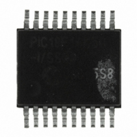
USB-DAQ-SS Flexipanel, USB-DAQ-SS Datasheet - Page 5

USB-DAQ-SS
Manufacturer Part Number
USB-DAQ-SS
Description
IC SYSTEM DATA LOGGER 20-SSOP
Manufacturer
Flexipanel
Datasheet
1.USB-DAQ-SS.pdf
(8 pages)
Specifications of USB-DAQ-SS
Lead Free Status / RoHS Status
Lead free / RoHS Compliant
Other names
658-1042-5
USB connector. C7 should be placed near the Vss and
Vdd pins of the USB-DAQ and is required only if it would
be some distance from C6. C8 is a filter capacitor for an
internal regulator and is required.
The TEAclipper connector is for in-circuit programming.
It is recommended to allow firmware updates, even if the
firmware is initially supplied pre-programmed. See the
TEAclipper programming section for details.
R3 pulls USB-S low when the USB connector is not
attached to a PC. R7 ensures the current is limited if
Vdd is below the USB supply voltage. Note how SCK-M
is biased low by R40. It must be low at startup, but may
otherwise be used as general I/O, as may the other
serial memory pins.
The OSCA and OSCB pins are not connected. There is
no real time clock and the event loop can only be
triggered by interrupt events.
Figure 4 shows a more advanced circuit with many
additional options added.
SW1 acts as a media detect switch for an SD card. If
25AA1024 memory is used, the Media input should
instead be biased low; if non-removable SD memory is
used, the Media input should instead be biased high.
Vto is gated by P-channel mosfet T1 to provide power
take-off circuit, for example to provide power to a battery
charger. C4 and R6 ensure the inrush current is not so
great as to cause a significant voltage drop.
In this circuit, two power sources are available: power
from the USB power input, and a battery Vbatt. D1 and
D2 ensure the higher of these is used by Vdd. If the
serial memory cannot not operate at 5V, the USB power
should be regulated to 3.3V.
X2, C4 and C5 comprise a real time clock oscillator.
LED1 shows a typical LED indicator circuit.
p5 of 8
C8
Vdd
Vss
Figure 3. Typical Application Circuit, Internal Memory
C7
Vusb
Vss
TEAclipper
connector
C6
R40
C1
USB-DAQ
1
26-Aug-10
2
3
R2
4
5
General I/O
Vss
External memory is used.
OSCA2
OSCA1
USB-S
D+
D-
Vss
X1
R3
C3
C2
Vss
R7
USB-DAQ
Vss
4
3
2
1
USB
USB Connectors
Common USB connector and cable configurations are
shown in figure 5 and table 6.
connector should be left unconnected. The ID pin on
the mini connector permits the distinction of A and B
plugs. The micro connector pin-out is the same as the
mini connector.
For ultra-low cost products, it is possible to form a USB
Type-A plug direct from a circuit board as shown in
figure 6. This connector is only suitable for a limited
number of insertions (~50 before cleaning is required).
It is unshielded and recommended only for ‘dongle’ type
products with no cables attached.
Std Mini
1
2
3
–
4
D1 and D2 should have a very low forward voltage – ideally 0.3V.
Pin
T1
Vdd
Vto
1
2
3
4
5
Figure 4. Typical Application Circuit, External Memory
R1
Figure 5 Common USB pin-outs for male connectors
Name
Vdd
Gnd
Vss
C8
Vcc
D+
D–
ID
Vdd
Vss
HW147-5
C9
Vdd
Vdd
Vdd
Vdd
R6
Table 6. USB Connection Key
PTO#
R40-R43
Gnd
C7
Vcc
Vusb
Cable
Green
color
White
Black
TEAclipper
Red
connector
C6
–
Memory
Serial
C1
1
USB-DAQ
2
SW1
Description
+5V (can dip to 4.08V)
Data –
Data +
Type A: Connect to ground
Type B: Not connected
Signal ground
3
R2
4
5
General I/O
Vss
OSCB2
OSCB1
OSCA2
OSCA1
USB-S
TxRx
The shield on the
D+
D-
Vss
R21
www.hexwax.com
C3
R3
X2
X1
C5
C2
LED1
Vdd
C4
Vss
D2
D1
Vss
Vss
Vss
Vbatt
4
3
2
1
USB


