ADUM7440ARQZ Analog Devices Inc, ADUM7440ARQZ Datasheet - Page 5
ADUM7440ARQZ
Manufacturer Part Number
ADUM7440ARQZ
Description
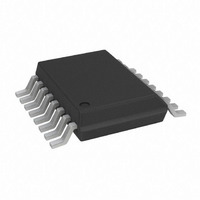
IC ISOLATOR DGTL QUAD 16QSOP
Manufacturer
Analog Devices Inc
Series
iCoupler®r
Datasheet
1.ADUM7441ARQZ.pdf
(20 pages)
Specifications of ADUM7440ARQZ
Propagation Delay
75ns
Inputs - Side 1/side 2
4/0
Number Of Channels
4
Isolation Rating
1000Vrms
Voltage - Supply
3 V ~ 5.5 V
Data Rate
1Mbps
Output Type
Logic
Package / Case
16-QSOP
Operating Temperature
-40°C ~ 105°C
No. Of Channels
4
Supply Current
4.3mA
Supply Voltage Range
3V To 5.5V
Digital Ic Case Style
QSOP
No. Of Pins
16
Operating Temperature Range
-40°C To +105°C
Lead Free Status / RoHS Status
Lead free / RoHS Compliant
Available stocks
Company
Part Number
Manufacturer
Quantity
Price
Company:

Part Number:
ADUM7440ARQZ
Manufacturer:
ADI
Quantity:
15
Part Number:
ADUM7440ARQZ
Manufacturer:
ADI/亚德诺
Quantity:
20 000


ELECTRICAL CHARACTERISTICS—MIXED 5 V/3.3 V OPERATION
All typical specifications are at T
mended operation range of 4.5 V ≤ V
specifications are tested with C
Table 7.
Parameter
SWITCHING SPECIFICATIONS
1
Table 8.
Parameter
SUPPLY CURRENT
Table 9. For All Models
Parameter
DC SPECIFICATIONS
AC SPECIFICATIONS
1
t
within the recommended operating conditions.
|CM| is the maximum common-mode voltage slew rate that can be sustained while maintaining V
rising and falling common-mode voltage edges.
PSK
ADuM7440
ADuM7441
ADuM7442
Data Rate
Propagation Delay
Pulse Width Distortion
Pulse Width
Propagation Delay Skew
Channel Matching
Jitter
Logic High Input Threshold
Logic Low Input Threshold
Logic High Output Voltages
Logic Low Output Voltages
Input Current per Channel
Supply Current per Channel
Output Rise/Fall Time
Common-Mode Transient Immunity
Refresh Rate
is the magnitude of the worst-case difference in t
Change vs. Temperature
Codirectional
Opposing-Direction
Quiescent Input Supply Current
Quiescent Output Supply Current
Dynamic Input Supply Current
Dynamic Output Supply Current
Symbol
I
I
I
I
I
I
1
DD1
DD2
DD1
DD2
DD1
DD2
L
= 15 pF and CMOS signal levels, unless otherwise noted.
A
= 25°C, V
Symbol
t
PWD
PW
t
t
t
PHL
PSK
PSKCD
PSKOD
DD1
1
t
Min
≤ 5.5 V, 3.0 V ≤ V
PLH
DD1
PHL
1 Mbps—A, C Grades
Symbol
V
V
V
V
I
I
I
I
I
t
|CM|
f
I
DDI(Q)
DDO(Q)
DDI(D)
DDO(D)
r
R
or t
IH
IL
OH
OL
/t
= 5 V, V
F
Min
250
PLH
4.4
1.6
3.7
2.2
3.2
2.0
Typ
that is measured between units at the same operating temperature, supply voltages, and output load
DD2
A Grade
0.7 V
V
Min
V
−10
15
DDx
Typ
55
10
5
2
DDx
DD2
= 3.3 V. Minimum/maximum specifications apply over the entire recom-
− 0.4
Rev. B | Page 5 of 20
− 0.1
DDx
≤ 3.6 V; and −40°C ≤ T
5.5
2.1
5.0
2.8
3.9
2.6
Max
Max
1
80
25
20
25
30
Typ
V
0.0
0.2
+0.01
0.77
0.40
0.26
0.02
2.5
20
1.2
V
DDx
DDx
− 0.2
Min
Min
30
40
25 Mbps—C Grade
O
C Grade
> 0.8 V
0.3 V
0.1
Max
0.4
+10
Typ
42
2
3
2
3
2
ADuM7440/ADuM7441/ADuM7442
A
28
3.5
19
5.2
15
7.8
Typ
≤ +105°C, unless otherwise noted. Switching
DDx
DD
. The common-mode voltage slew rates apply to both
Max
25
55
5
10
5
6
Unit
V
V
V
V
V
V
µA
mA
mA
mA/Mbps
mA/Mbps
ns
kV/µs
Mbps
35
4.5
27
7.0
20
12
Max
Unit
Mbps
ns
ns
ps/°C
ns
ns
ns
ns
ns
mA
mA
mA
mA
mA
mA
Unit
transient magnitude = 800 V
Test Conditions
I
I
I
I
0 V ≤ V
10% to 90%
V
Ox
Ox
Ox
Ox
Test Conditions
Within PWD limit
50% input to 50% output
|t
Within PWD limit
Ix
PLH
= −20 µA, V
= −4 mA, V
= 20 µA, V
= 4 mA, V
= V
− t
DDx
Ix
Test Conditions
≤ V
PHL
, V
DDx
|
CM
Ix
Ix
Ix
= 1000 V,
= V
Ix
= V
= V
= V
IxL
IxL
IxH
IxH
Related parts for ADUM7440ARQZ
Image
Part Number
Description
Manufacturer
Datasheet
Request
R

Part Number:
Description:
±1.7g Dual-Axis IMEMS Accelerometer Evaluation Board
Manufacturer:
Analog Devices Inc
Datasheet:

Part Number:
Description:
Inertial Sensor Evaluation System
Manufacturer:
Analog Devices Inc
Datasheet:
Part Number:
Description:
Manufacturer:
Analog Devices Inc
Datasheet:
Part Number:
Description:
Manufacturer:
Analog Devices Inc
Datasheet:
Part Number:
Description:
Manufacturer:
Analog Devices Inc
Datasheet:
Part Number:
Description:
Manufacturer:
Analog Devices Inc
Datasheet:
Part Number:
Description:
Manufacturer:
Analog Devices Inc
Datasheet:
Part Number:
Description:
Manufacturer:
Analog Devices Inc
Datasheet:
Part Number:
Description:
Manufacturer:
Analog Devices Inc
Datasheet:
Part Number:
Description:
Manufacturer:
Analog Devices Inc
Datasheet:
Part Number:
Description:
Manufacturer:
Analog Devices Inc
Datasheet:
Part Number:
Description:
Manufacturer:
Analog Devices Inc
Datasheet:
Part Number:
Description:
Manufacturer:
Analog Devices Inc
Datasheet: