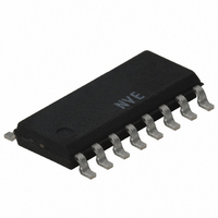
IL260-3E NVE, IL260-3E Datasheet - Page 5

IL260-3E
Manufacturer Part Number
IL260-3E
Description
ISOLATOR HS 5CHAN DIGITAL 16SOIC
Manufacturer
NVE
Series
IsoLoop®r
Datasheet
1.IL260E.pdf
(11 pages)
Specifications of IL260-3E
Inputs - Side 1/side 2
5/0
Number Of Channels
5
Isolation Rating
2500Vrms
Voltage - Supply
3 V ~ 5.5 V
Data Rate
110Mbps
Propagation Delay
12ns
Output Type
CMOS
Package / Case
16-SOIC (3.9mm Width)
Operating Temperature
-40°C ~ 85°C
No. Of Channels
5
Supply Current
300µA
Supply Voltage Range
3V To 5.5V
Digital Ic Case Style
SOIC
No. Of Pins
16
Operating Temperature Range
-40°C To +85°C
Lead Free Status / RoHS Status
Lead free / RoHS Compliant
Other names
390-1069-5
Available stocks
Company
Part Number
Manufacturer
Quantity
Price
Part Number:
IL260-3E
Manufacturer:
NEV
Quantity:
20 000
5 Volt Electrical Specifications (T
Notes (apply to both 3.3 V and 5 V specifications):
1.
2.
3.
4.
5.
6.
7.
8.
9.
10. 66,535-bit pseudo-random binary signal (PRBS) NRZ bit pattern with no more than five consecutive 1s or 0s; 800 ps transition time.
Parameters
Input Quiescent Current
Output Quiescent Current
Logic Input Current
Logic High Output Voltage
Logic Low Output Voltage
Maximum Data Rate
Minimum Pulse Width
Propagation Delay Input to Output
(High to Low)
Propagation Delay Input to Output
(Low to High)
Pulse Width Distortion |t
Pulse Jitter
Propagation Delay Skew
Output Rise Time (10%–90%)
Output Fall Time (10%–90%)
Common Mode Transient Immunity
(Output Logic High to Logic Low)
Channel-to-Channel Skew
Dynamic Power Consumption
Power Frequency Magnetic Immunity
Pulse Magnetic Field Immunity
Damped Oscillatory Magnetic Field
Cross-axis Immunity Multiplier
Absolute maximum ambient operating temperature means the device will not be damaged if operated under these conditions. It does not
guarantee performance.
PWD is defined as |t
t
CM
common mode input voltage that can be sustained while maintaining V
and falling common mode voltage edges.
Device is considered a two terminal device: pins 1–8 shorted and pins 9–16 shorted.
Dynamic power consumption numbers are calculated per channel and are supplied by the channel’s input side power supply.
Minimum pulse width is the minimum value at which specified PWD is guaranteed.
The relevant test and measurement methods are given in the Electromagnetic Compatibility section on p. 6.
External magnetic field immunity is improved by this factor if the field direction is “end-to-end” rather than to “pin-to-pin” (see diagram on p. 6).
PSK
is the magnitude of the worst-case difference in t
H
is the maximum common mode voltage slew rate that can be sustained while maintaining V
(10)
(7)
PHL
PHL
(3)
− t
−t
PLH
PLH
(6)
IL260
IL261
IL262
IL260
IL261
IL262
(9)
|
(2)
|. %PWD is equal to PWD divided by pulse width.
(4)
min
Magnetic Field Immunity
|CM
to T
Symbol
PWD
H
I
I
V
V
H
PW
t
t
t
H
H
K
DD1
DD2
PHL
PLH
PSK
t
t
t
|,|CM
OSC
I
OH
OL
R
PM
max
F
PF
J
i
X
)
L
PHL
|
Switching Specifications
and/or t
0.8 x V
V
Min.
DD
2800
4000
4000
−10
100
10
20
PLH
−0.1
DD
(8)
between devices at 25°C.
5
(V
O
DD2
< 0.8 V. The common mode voltage slew rates apply to both rising
0.9 x V
= 5V, 3V<V
Typ.
3500
4500
4500
V
350
110
100
200
2.5
7.5
0.5
2.5
10
10
10
30
5
5
0
2
4
1
1
2
DD
DD
DD1
Max.
<5.5V)
500
340
0.1
0.8
IL260/IL261/IL262
15
12
10
15
15
3
6
9
3
6
3
3
3
O
> 0.8 V
μA/MHz
kV/μs
Units
Mbps
A/m
A/m
A/m
mA
mA
mA
mA
mA
μA
μA
ns
ns
ns
ns
ps
ns
ns
ns
ns
DD
V
V
2
. CM
L
is the maximum
Test Conditions
I
I
I
I
C
50% Points, V
C
C
C
C
C
C
C
V
C
per channel
50Hz/60Hz
t
0.1Hz – 1MHz
p
O
O
O
O
L
L
L
L
L
L
L
L
L
CN
= 8µs
= −20 μA, V
= −4 mA, V
= 20 μA, V
= 4 mA, V
= 15 pF
= 15 pF
= 15 pF
= 15 pF
= 15 pF
= 15 pF
= 15 pF
= 15 pF
= 15 pF
= 300 V
I
I
= V
O
I
= V
I
= V
= V
IL
IL
IH
IH


