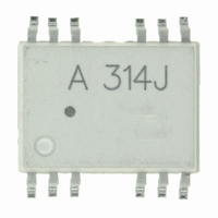
HCPL-314J-000E Avago Technologies US Inc., HCPL-314J-000E Datasheet - Page 5

HCPL-314J-000E
Manufacturer Part Number
HCPL-314J-000E
Description
OPTOCOUPLER GATE DRV 0.4A 16SOIC
Manufacturer
Avago Technologies US Inc.
Datasheet
1.HCPL-314J-000E.pdf
(14 pages)
Specifications of HCPL-314J-000E
Package / Case
16-SOIC (0.300", 7.50mm Width)
Voltage - Isolation
3750Vrms
Number Of Channels
2, Unidirectional
Propagation Delay High - Low @ If
300ns @ 8mA
Current - Dc Forward (if)
25mA
Input Type
DC
Output Type
Open Collector
Mounting Type
Surface Mount
Isolation Voltage
3750 Vrms
Maximum Fall Time
0.05 us
Maximum Forward Diode Current
25 mA
Minimum Forward Diode Voltage
1.2 V
Output Device
Logic Gate Photo IC
Configuration
2 Channel
Maximum Forward Diode Voltage
1.8 V
Maximum Reverse Diode Voltage
3 V
Maximum Power Dissipation
260 mW
Maximum Operating Temperature
+ 100 C
Minimum Operating Temperature
- 40 C
No. Of Channels
2
Optocoupler Output Type
Gate Drive
Input Current
12mA
Output Voltage
30V
Opto Case Style
SOIC
No. Of Pins
16
Common Mode Ratio
10 KV/uS
Rohs Compliant
Yes
Lead Free Status / RoHS Status
Lead free / RoHS Compliant
Lead Free Status / RoHS Status
Lead free / RoHS Compliant, Lead free / RoHS Compliant
Other names
516-1477-5
Available stocks
Company
Part Number
Manufacturer
Quantity
Price
Company:
Part Number:
HCPL-314J-000E
Manufacturer:
AVAGO
Quantity:
4 000
Company:
Part Number:
HCPL-314J-000E
Manufacturer:
AVAGO
Quantity:
30 000
Electrical Specifications (DC)
Over recommended operating conditions unless otherwise specified.
Switching Specifications (AC)
Over recommended operating conditions unless otherwise specified.
5
Parameter
High Level Output Current
Low Level Output Current
High Level Output Voltage
Low Level Output Voltage
High Level Supply Current
Low Level Supply Current
Threshold Input Current
Low to High
Threshold Input Voltage
High to Low
Input Forward Voltage
Temperature Coefficient
of Input Forward Voltage
Input Reverse Breakdown
Voltage
Input Capacitance
Parameter
Propagation Delay Time
to High Output Level
Propagation Delay Time
to Low Output Level
Propagation Delay
Difference Between Any
Two Parts or Channels
Rise Time
Fall Time
Output High Level Common
Mode Transient Immunity
Output Low Level Common
Mode Transient Immunity
Symbol
I
I
V
V
I
I
I
V
V
'V
BV
C
OH
OL
CCH
CCL
FLH
Symbol
t
t
PDD
t
t
|CM
|CM
OH
OL
FHL
F
IN
PLH
PHL
R
F
R
F
/'T
H
L
|
|
A
Min.
0.2
0.2
V
0.8
1.2
3
Min.
0.1
0.1
-0.5
25
25
CC
-4
Typ.
0.4
0.4
0.4
V
0.4
0.7
1.2
1.5
-1.2
10
70
Typ.
0.2
0.3
50
50
35
35
CC
-1.8
Max.
0.7
0.7
0.5
Max.
0.5
0.5
1
3
3
5
1.8
Units
μs
μs
μs
ns
ns
kV/μs
kV/μs
Units
A
A
V
V
mA
mA
mA
V
V
mV/°C
V
pF
Test Conditions
Vo = V
Vo = V
Vo = V
Vo = V
Io = -100 mA
Io = 100 mA
Io = 0 mA
Io = 0 mA
Io = 0 mA, Vo>5 V
I
I
f = 1 MHz,
V
F
R
Test Conditions
Rg = 47 Ω,
Cg = 3 nF,
f = 10 kHz,
Duty Cycle =50%,
I
V
T
V
F
F
A
= 10 mA
= 100 μA
CC
CM
= 0 V
= 8 mA,
= 25°C,
= 30 V
= 1.5 kV
CC
CC
EE
EE
+2.5
+10
- 4
-10
Fig.
10, 11,
12, 13,
14, 17
18
18
Fig.
2
3
5
6
1
4
7, 8
9, 15
16
Note
14
10
11,
12
11,
13
Note
5
2
5
2
6, 7
15


