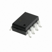
HCPL-7723-300 Avago Technologies US Inc., HCPL-7723-300 Datasheet - Page 6

HCPL-7723-300
Manufacturer Part Number
HCPL-7723-300
Description
OPTOCOUPLER CMOS 50MBD GW 8-SMD
Manufacturer
Avago Technologies US Inc.
Datasheet
1.HCPL-7723-300.pdf
(12 pages)
Specifications of HCPL-7723-300
Voltage - Isolation
3750Vrms
Number Of Channels
1, Unidirectional
Current - Output / Channel
10mA
Data Rate
50MBd
Propagation Delay High - Low @ If
16ns
Input Type
Logic
Output Type
Push-Pull, Totem-Pole
Mounting Type
Surface Mount, Gull Wing
Package / Case
8-SMD Gull Wing
No. Of Channels
1
Isolation Voltage
3.75kV
Optocoupler Output Type
Logic Gate
Input Current
10µA
Output Voltage
5V
Opto Case Style
SMD
No. Of Pins
8
Propagation Delay Low-high
22ns
Common Mode Voltage Vcm
1000V
Number Of Elements
1
Baud Rate
50Mbps
Output Current
10mA
Package Type
PDIP SMD
Operating Temp Range
-40C to 85C
Power Dissipation
150mW
Propagation Delay Time
22ns
Pin Count
8
Mounting
Surface Mount
Operating Temperature Classification
Industrial
Lead Free Status / RoHS Status
Contains lead / RoHS non-compliant
Lead Free Status / RoHS Status
Contains lead / RoHS non-compliant, Contains lead / RoHS non-compliant
Other names
516-1108-5
All Avago data sheets report the creepage and clearance
inherent to the optocoupler component itself. These
dimensions are needed as a starting point for the
equipment designer when determining the circuit insula-
tion requirements. However, once mounted on a printed
circuit board, minimum creepage and clearance require-
ments must be met as specified for individual equipment
standards. For creepage, the shortest distance path along
IEC/EN/DIN EN 60747-5-2 Insulation Related Characteristics (Option 060)
Description
Installation classification per DIN VDE 0110/1.89, Table 1
Climatic Classification
Pollution Degree (DIN VDE 0110/1.89)
Maximum Working Insulation Voltage
Input to Output Test Voltage, Method b*
Input to Output Test Voltage, Method a*
Highest Allowable Overvoltage*
(Transient Overvoltage, t
Safety Limiting Values (maximum values allowed in the
event of a failure, also see Thermal Derating curve,
Figure 11)
Insulation Resistance at T
*Refer to the front of the optocoupler section of the Isolation and Control Component Designer’s Catalog, under Product Safety Regulations sec-
tion IEC/EN/DIN EN 60747-5-2, for a detailed description.
Note: These optocouplers are suitable for “safe electrical isolation” only within the safety limit data. Maintenance of the safety data shall be en-
sured by means of protective circuits.
Note: The surface mount classification is Class A in accordance with CECC 00802.
6
V
V
for rated mains voltage ≤ 150 V rms
for rated mains voltage ≤ 300 V rms
for rated mains voltage ≤ 450 V rms
Partial Discharge
Partial Discharge
Case Temperature
Input Current
Output Power
IORM
IORM
x 1.875 = V
x 1.5 = V
PR
< 5 pC
, Type and Sample Test, t
< 5 pC
PR
, 100% Production Test with t
ini
S
, V
= 10 sec)
IO
= 500 V
m
= 60 sec,
m
= 1 sec,
the surface of a printed circuit board between the solder
fillets of the input and output leads must be considered.
There are recommended techniques such as grooves
and ribs, which may be used on a printed circuit board
to achieve desired creepage and clearances. Creepage
and clearance distances will also change depending on
factors such as pollution degree and insulation level.
Symbol
V
V
V
V
T
I
P
R
S,INPUT
S
IORM
PR
PR
S,OUTPUT
IOTM
IO
HCPL-7723
Option 060
I-IV
I-IV
I-III
55/85/21
2
630
1181
945
6000
175
230
600
≥ 10
9
HCPL-0723
Option 060
I-IV
I-III
55/85/21
2
560
1050
840
4000
150
150
600
≥ 10
9
Units
V peak
V peak
V peak
V peak
°C
mA
mW
Ω


