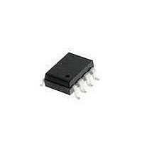
HCPL-2411#500 Avago Technologies US Inc., HCPL-2411#500 Datasheet - Page 10

HCPL-2411#500
Manufacturer Part Number
HCPL-2411#500
Description
ISOLAT 2.5KVRMS 1CH UNIDIR 8SMD
Manufacturer
Avago Technologies US Inc.
Datasheet
1.HCPL-2400-300E.pdf
(15 pages)
Specifications of HCPL-2411#500
Package / Case
8-SMD Gull Wing
Voltage - Isolation
2500Vrms
Number Of Channels
1, Unidirectional
Current - Output / Channel
25mA
Data Rate
40MBd
Propagation Delay High - Low @ If
33ns @ 7mA
Current - Dc Forward (if)
10mA
Input Type
DC
Output Type
Open Collector
Mounting Type
Surface Mount, Gull Wing
Isolation Voltage
2500 Vrms
Maximum Continuous Output Current
25 mA
Maximum Fall Time
10 ns
Maximum Forward Diode Current
10 mA
Maximum Rise Time
20 ns
Minimum Forward Diode Voltage
1.1 V
Output Device
Logic Gate Photo IC
Configuration
1 Channel
Maximum Baud Rate
40 MBps
Maximum Forward Diode Voltage
1.5 V
Maximum Reverse Diode Voltage
3 V
Maximum Power Dissipation
40 mW
Maximum Operating Temperature
+ 70 C
Minimum Operating Temperature
0 C
Lead Free Status / RoHS Status
Contains lead / RoHS non-compliant
Available stocks
Company
Part Number
Manufacturer
Quantity
Price
10
Package Characteristics
*All typical values are at T
**The Input-Output Momentary Withstand Voltage is a dielectric voltage rating that should not be interpreted as an input-output continuous
voltage rating. For the continuous voltage rating refer to the VDE 0884 Insulation Related Characteristics Table (if applicable), your equipment lev-
el safety specification or Avago Application Note 1074 entitled “Optocoupler Input-Output Endurance Voltage, ” publication number 5963-2203E.
Notes:
10. Power Supply Noise Immunity is the peak to peak amplitude of the ac ripple voltage on the V
11. Use of a 0.1 µF bypass capacitor connected between pins 8 and 5 adjacent to the device is required.
12. Peak Forward Input Current pulse width < 50 µs at 1 KHz maximum repetition rate.
13. In accordance with UL 1577, each optocoupler is proof tested by applying an insulation test voltage ≥ 4500 V rms for one second (leakage detec-
1. Each channel.
2. Duration of output short circuit time not to exceed 10 ms.
3. Device considered a two terminal device: pins 1, 2, 3, and 4 shorted together, and pins 5, 6, 7, and 8 shorted together.
4. t
5. The typical data shown is indicative of what can be expected using the application circuit in Figure 13.
6. This specification simulates the worst case operating conditions of the HCPL-2400 over the recommended operating temperature and V
7. Propagation delay skew is discussed later in this data sheet.
8. Measured between pins 1 and 2 shorted together, and pins 3 and 4 shorted together.
9. Common mode transient immunity in a Logic High level is the maximum tolerable (positive) dV
Parameter
Input-Output
Momentary
Withstand Voltage**
Input-Output
Resistance
Input-Output
Capacitance
Input-Input
Insulation Leakage
Current
Resistance
(Input-Input)
Capacitance
(Input-Input)
output pulse. The t
rising edge of the output pulse.
with the suggested application circuit of Figure 13.
that the output will remain in a Logic High state (i.e., V
able (negative) dV
in the desired logic state. For desired logic high state, V
tion current limit, I
Characteristics Table, if applicable.
PHL
propagation delay is measured from the 50% level on the rising edge of the input current pulse to the 1.5 V level on the falling edge of the
CM
I-O
PLH
/dt of the common mode pulse, V
≤ 5 µA). This test is performed before the 100% Production test shown in the IEC/EN/DIN EN 60747-5-2 Insulation Related
A
propagation delay is measured from the 50% level on the falling edge of the input current pulse to the 1.5 V level on the
= 25°C.
Sym.
V
R
C
C
R
I
ISO
I-I
I-O
I-O
I-I
I-I
Device
2430
2430
2430
CM
3750
O
Min.
OH(MIN)
, to assure that the output will remain in a Logic Low state (i.e., V
> 2.0 V). Common mode transient immunity in a Logic Low level is the maximum toler-
> 2.0 V, and for desired logic low state, V
0.005
Typ.*
0.25
10
10
0.6
12
11
Max.
Units
V rms
µA
pF
pF
Ω
Ω
CC
line that the device will withstand and still remain
Test Conditions
CM
/dt of the common mode pulse, V
RH ≤50%,
t = 1 min.,
T
V
f = 1 MHz
V
RH ≤45%
t = 5 s,
V
V
f = 1 MHz
A
I-O
I-O
I-I
I-I
= 25°C
OL(MAX)
= 500 Vdc
= 500 Vdc
= 500 Vdc
= 0 Vdc
< 0.8 V.
O
< 0.8 V).
Fig.
CM
, to assure
3, 13
Note
CC
3
8
8
8
range


