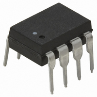
HCPL-3100 Avago Technologies US Inc., HCPL-3100 Datasheet

HCPL-3100
Specifications of HCPL-3100
Available stocks
Related parts for HCPL-3100
HCPL-3100 Summary of contents
Page 1
... The HCPL-3100 switches a 3000 pF load and the HCPL-3101, using a higher speed LED, switches a 3000 pF load in 0.5 s. With a CMR rating of 15 kV/ s typical these opto-couplers readily reject transients found in inverter applications ...
Page 2
... To order, choose a part number from the part number column and combine with the desired option from the option column to form an order entry. Example 1: HCPL-3100-500E to order product of 300 mil DIP Gull Wing Surface Mount package in Tape and Reel packaging and RoHS compliant. Example 2: HCPL-3101-000E to order product of 300 mil DIP package in Tube packaging and RoHS compliant ...
Page 3
... DATE CODE YYWW 9.16 (0.361) 10.16 (0.400) 0.50 (0.020) TYP. 2.90 (0.114) 3.90 (0.154) 2.29 (0.090) 2.79 (0.110) 3 6.00 (0.236) 7.32 (0.288) 7.00 (0.276) 7.92 (0.312) HCPL-3100 ANODE CATHODE 2 7 GND Q2 3.00 (0.118) 4.00 (0.157 2.55 (0.100) 3.55 (0.140) 0.40 (0.016) ...
Page 4
... I O2 Current Peak Current Output Power Dissipation P Total Power Dissipation P Lead Solder Temperature 4 Regulatory Information The HCPL-3100/3101 has been approved by the following organization: UL Recognized under UL 1577, Component Recognition Program, File E55361. Value Units 6.0 mm Shortest distance measured through air, between two conductive leads, input to output 6 ...
Page 5
... Recommended Operating Conditions Parameter Symbol Power Supply Voltage Input Current (ON) Operating Temperature Recommended Protection for Output Transistors During switching transitions, the output transistors Q1 and Q2 of the HCPL-3100/3101 can conduct large amounts of current. Figure 1 describes ANODE CONTROL TTL OR CATHODE LSTTL INPUT TOTEM ...
Page 6
... Electrical Specifications Over recommended temperature ( +100 C, HCPL-3100 Parameter Sym. Device Input Forward V HCPL-3100 F Voltage HCPL-3101 Input Reverse I HCPL-3100 R Current HCPL-3101 Input Capacitance C HCPL-3100 IN HCPL-3101 Output 1 Low V HCPL-3100 O1L Level Voltage HCPL-3101 Leakage I O1L Current Output 2 High V HCPL-3100 O2H Level Voltage HCPL-3101 ...
Page 7
... HCPL-3100 PHL Delay Time to Low Output HCPL-3101 Level Rise Time t HCPL-3100 r HCPL-3101 Fall Time t HCPL-3100 f HCPL-3101 Output High |CM | HCPL-3100 H Level Common Mode Transient HCPL-3101 Immunity Output Low | Level Common Mode Transient Immunity Packaging Characteristics Parameter Sym. Input-Output Momentary V ISO Withstand Voltage* ...
Page 8
... CC2 - – O1L + . Figure 3. Test circuit for high level output voltage V O1L + – I O2L Figure 5. Test circuit for leakage current I O2L + Figure 7. Test circuit for – FLH HCPL-3100 GND – O2H + O2H HCPL-3100 GND O1L O1L HCPL-3100 GND and I . CCH CCL ...
Page 9
... Figure 9. Test circuit for and t . PLH PHL -40 - 100 125 AMBIENT TEMPERATURE Figure 11. LED forward current vs. ambient temperature, HCPL-3100 – mA, HCPL-3100 mA, HCPL-3101 F 10 Figure 10. Test circuit for -40 - 100 AMBIENT TEMPERATURE Figure 12. LED forward current vs. ambient temperature, HCPL-3101. HCPL-3100 GND 2 7 – – ...
Page 10
... AMBIENT TEMPERATURE Figure 14. Maximum power dissipation vs. ambient temperature, HCPL-3101. 120 110 VALUE ASSUME 100 100 SUPPLY VOLTAGE V (V) CC Figure 17. Normalized low to high threshold input current vs. supply voltage, HCPL-3100. 120 110 100 I = 100 FLH -40 - 100 AMBIENT TEMPERATURE Figure 20. Normalized low to high threshold input current vs ...
Page 11
... CC Figure 26. Typical high level output 2 voltage vs. supply voltage, HCPL-3101 0.1 0.2 0.3 0.4 0.5 0.6 O OUTPUT CURRENT I ( Figure 29. Typical low level output 2 voltage vs. output 2 current, HCPL-3100 CC1 V = -12 V CC2 0. 0 0.20 0.15 0.10 0.05 0 -40 - 100 AMBIENT TEMPERATURE Figure 24. Typical low level output 1 voltage vs ...
Page 12
... Figure 34. Typical high level supply current vs. supply voltage, HCPL-3101 2.0 1.5 1.0 0.5 0 -40 - 100 AMBIENT TEMPERATURE Figure 37. Typical high level supply current vs. ambient temperature, HCPL-3100 2.0 1.5 1.0 0.5 0 -40 - 100 AMBIENT TEMPERATURE Figure 40. Typical low level supply current vs. ambient temperature, HCPL-3101. ...
Page 13
... Figure 44. Typical propagation delay time vs. ambient temperature, HCPL-3101. 13 1.0 t PHL PLH 0 3000 0 FORWARD CURRENT I (mA) F Figure 42. Typical propagation delay time vs. forward current, HCPL-3101 3000 1.5 1.0 t PHL 0.5 t PLH 0 -40 - 100 AMBIENT TEMPERATURE Figure 43. Typical propagation delay time vs. ambient temperature, HCPL-3100. ...
Page 14
For product information and a complete list of distributors, please go to our website: Avago, Avago Technologies, and the A logo are trademarks of Avago Technologies Limited in the United States and other countries. Data subject to change. Copyright © ...


