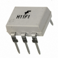
H11F1M Fairchild Optoelectronics Group, H11F1M Datasheet

H11F1M
Specifications of H11F1M
Available stocks
Related parts for H11F1M
H11F1M Summary of contents
Page 1
... CATHODE 2 3 ©2007 Fairchild Semiconductor Corporation H11F1M, H11F2M, H11F3M Rev. 1.0.4 General Description The H11FXM series consists of a Gallium-Aluminum- Arsenide IRED emitting diode coupled to a symmetrical bilateral silicon photo-detector. The detector is electri- cally isolated from the input and performs like an ideal isolated FET designed for distortion-free control of low level AC and DC analog signals ...
Page 2
... DETECTOR P Detector Power Dissipation @ 25°C D Derate linearly from 25°C BV Breakdown Voltage (either polarity) 4-6 I Continuous Detector Current (either polarity) 4-6 ©2007 Fairchild Semiconductor Corporation H11F1M, H11F2M, H11F3M Rev. 1.0 25°C unless otherwise specified) A Device H11F1M, H11F2M H11F3M 2 Value Units All -40 to +150 ° ...
Page 3
... Isolation Characteristics Symbol Characteristic V Isolation Voltage ISO R Isolation Resistance ISO C Isolation Capacitance ISO *All Typical values 25°C A ©2007 Fairchild Semiconductor Corporation H11F1M, H11F2M, H11F3M Rev. 1.0 25°C unless otherwise specified.) A Test Conditions Device I = 16mA All All 1.0MHz All I = 10µA, I ...
Page 4
... Max. Working Insulation Voltage IORM V Highest Allowable Over Voltage IOTM External Creepage External Clearance Insulation Thickness RIO Insulation Resistance at Ts, V ©2007 Fairchild Semiconductor Corporation H11F1M, H11F2M, H11F3M Rev. 1.0.4 Parameter , 100% Production Test PR , Type and Sample Test = 500V IO 4 Min. Typ. Max. ...
Page 5
... 1.2 1 100 C A 0.8 0 – LED FOR WARD CURRENT (mA) F ©2007 Fairchild Semiconductor Corporation H11F1M, H11F2M, H11F3M Rev. 1.0.4 800 600 400 200 0 -200 -400 -600 -800 100 Figure 4. Off-state Current vs. Ambient Temperature 10000 1000 100 100 0 Figure 5. Resistive Non-Linearity vs. D.C. Bias ...
Page 6
... The linearity of resistance and the low offset voltage of the H11FXM allows the remote tuning or band-switching of active filters without switching glitches or distortion. This schematic illustrates the concept, with current to the H11F1M IRED’s controlling the filter’s transfer characteristic. ©2007 Fairchild Semiconductor Corporation H11F1M, H11F2M, H11F3M Rev ...
Page 7
... Note: All dimensions in mm. ©2007 Fairchild Semiconductor Corporation H11F1M, H11F2M, H11F3M Rev. 1.0.4 0.4" Lead Spacing 6.10–6.60 7.62 (Typ.) 5.08 (Max.) 0.38 (Min.) 0.20–0.30 15° (Typ.) (0.86) 1.02–1.78 8.13– ...
Page 8
... TV SV SR2V Marking Information Definitions ©2007 Fairchild Semiconductor Corporation H11F1M, H11F2M, H11F3M Rev. 1.0.4 (Example) H11F1M Standard Through Hole Device H11F1SM Surface Mount Lead Bend H11F1SR2M Surface Mount; Tape and Reel H11F1VM IEC60747-5-2 approval H11F1TVM IEC60747-5-2 approval, 0.4" Lead Spacing H11F1SVM ...
Page 9
... Carrier Tape Specification 4.5 0.20 0.30 21.0 0.1 0.1 MAX User Direction of Feed ©2007 Fairchild Semiconductor Corporation H11F1M, H11F2M, H11F3M Rev. 1.0.4 12.0 0.1 2.0 0.05 0.05 4.0 0.1 10.1 0.20 9 Ø1.5 MIN 1.75 0.10 11.5 1.0 24.0 0.3 9.1 0.20 Ø ...
Page 10
... Maintained Above (T L Peak Body Package Temperature Time (t ) within 5°C of 260°C P Ramp-down Rate (T Time 25°C to Peak Temperature ©2007 Fairchild Semiconductor Corporation H11F1M, H11F2M, H11F3M Rev. 1.0.4 Max. Ramp-up Rate = 3°C/S Max. Ramp-down Rate = 6°C/S Tsmax Preheat Area Tsmin t s 120 240 Time 25° ...
Page 11
... Datasheet Identification Product Status Advance Information Formative / In Design Preliminary First Production No Identification Needed Full Production Obsolete Not In Production ©2007 Fairchild Semiconductor Corporation H11F1M, H11F2M, H11F3M Rev. 1.0.4 ® PowerTrench ® PowerXS™ SM Programmable Active Droop™ ® QFET QS™ Quiet Series™ ...


