SFH6343T Vishay, SFH6343T Datasheet - Page 3
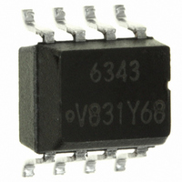
SFH6343T
Manufacturer Part Number
SFH6343T
Description
OPTOCOUPLER TRANS OUT 19% 8SOIC
Manufacturer
Vishay
Specifications of SFH6343T
Isolation Voltage
4 KV
Voltage - Isolation
4000Vrms
Number Of Channels
1, Unidirectional
Current - Output / Channel
8mA
Data Rate
1MBd
Current - Dc Forward (if)
25mA
Input Type
DC
Output Type
Open Collector
Mounting Type
Surface Mount
Package / Case
8-SOIC (3.9mm Width)
Voltage - Output
25V
Current Transfer Ratio (max)
50% @ 16mA
Current Transfer Ratio (min)
15% @ 16mA
Output Device
Transistor With Base
Configuration
1 Channel
Current Transfer Ratio
36 % (Typ)
Maximum Baud Rate
1 MBps
Maximum Forward Diode Voltage
1.8 V
Maximum Reverse Diode Voltage
3 V
Maximum Input Diode Current
25 mA
Maximum Power Dissipation
100 mW
Maximum Operating Temperature
+ 70 C
Minimum Operating Temperature
0 C
No. Of Channels
1
Optocoupler Output Type
Phototransistor
Input Current
16mA
Output Voltage
25V
Opto Case Style
SOIC
No. Of Pins
8
Propagation Delay Low-high
1µs
Approval Bodies
UL, CSA
Rohs Compliant
Yes
Lead Free Status / RoHS Status
Lead free / RoHS Compliant
Vce Saturation (max)
-
Lead Free Status / Rohs Status
Lead free / RoHS Compliant
Other names
751-1364-2
SFH6343TGITR
SFH6343TGITR
SFH6343TGITR
SFH6343TGITR
Available stocks
Company
Part Number
Manufacturer
Quantity
Price
Company:

Part Number:
SFH6343T
Manufacturer:
SIEMENS
Quantity:
5 510
Company:
Part Number:
SFH6343T
Manufacturer:
SIEMENS
Quantity:
5 510


Notes
• Minimum and maximum values are testing requirements. Typical values are characteristics of the device and are the result of engineering
(1)
Note
• Current transfer ratio in percent equals the ratio of output collector current (I
Notes
• Over recommended temperature (T
(1)
Document Number: 83677
Rev. 2.1, 19-Oct-10
ELECTRICAL CHARACTERISTICS (T
PARAMETER
COUPLER
Capacitance (input to output)
CURRENT TRANSFER RATIO
PARAMETER
Current transfer ratio
SWITCHING CHARACTERISTICS
PARAMETER
Propagation delay time to logic
low at output (see fig. 1)
Propagation delay time to logic
high at output (see fig. 1)
evaluation. Typical values are for information only and are not part of the testing requirements.
A 0.1 μF bypass capacitor connected between pins 5 and 8 is recommended.
A 0.1 μF bypass capacitor connected between pins 5 and 8 is recommended.
The 1.9 kW load represents 1 TTL unit load of 1.6 mA and the 5.6 kW pull-up resistor.
The 4.1 kW load represents 1 LSTTL unit load of 0.36 mA and the 6.1 kW pull-up resistor.
T
amb
= 25 °C, unless otherwise specified.
isfh6315t_01
10 % duty cycle
1/f < 100 µs
I
Pulse
generator
Z
t
F
r
O
= 5 ns
= monitor
= 50 Ω
R
I
F
M
(1)
4
1
2
3
V
V
V
V
V
V
O
O
O
For technical questions, contact:
O
O
O
amb
= 0.4 V, I
= 0.4 V, I
= 0.4 V, I
= 0.5 V, I
= 0.5 V, I
= 0.5 V, I
TEST CONDITION
= 0 °C to 70 °C ), V
TEST CONDITION
TEST CONDITION
R
R
R
R
High Speed Optocoupler, 1 MBd,
L
L
L
L
= 4.1 KΩ
= 1.9 KΩ
= 4.1 KΩ
= 1.9 KΩ
F
F
F
F
F
F
f = 1 MHz
= 16 mA, V
= 16 mA, V
= 16 mA, V
= 16 mA, V
= 16 mA, V
= 16 mA, V
25 °C
25 °C
25 °C
Fig. 1 - Test Circuit for Switching Times
amb
8
7
6
5
Transistor Output
= 25 °C, unless otherwise specified)
CC
CC
CC
CC
CC
CC
CC
0.1 µF
= 4.5 V,
= 4.5 V,
= 4.5 V,
= 4.5 V
= 4.5 V
= 4.5 V
= 5 V, I
R
SFH6315T
SFH6315T
SFH6316T
SFH6343T
SFH6315T
SFH6315T
SFH6316T
SFH6343T
L
PART
C
optocoupleranswers@vishay.com
L
F
SFH6315T, SFH6316T, SFH6343T
+ 5 V
= 15 pF
V
= 16 mA unless otherwise specified.
SFH6315T
SFH6315T
SFH6316T
SFH6343T
SFH6343T
SFH6316T
O
PART
PART
O
SYMBOL
) to the forward LED input current (I
V
t
t
I
0
PHL
PLH
F
O
t
t
t
t
t
t
PHL
PHL
PHL
PLH
PLH
PLH
t
PHL
(1)
(1)
SYMBOL
SYMBOL
CTR
CTR
CTR
CTR
CTR
CTR
C
IO
MIN.
1.5 V
Vishay Semiconductors
MIN.
MIN.
19
19
15
15
7
5
t
PLH
TYP.
0.25
0.25
0.5
0.5
0.5
0.5
0.5
0.5
TYP.
TYP.
0.4
16
17
35
35
36
36
F
1.5 V
) times 100.
MAX.
1.5
0.8
1.5
0.8
MAX.
V
MAX.
2
1
2
1
5 V
OL
50
50
50
www.vishay.com
UNIT
UNIT
UNIT
μs
μs
μs
μs
μs
μs
μs
μs
pF
%
%
%
%
%
%
3
Related parts for SFH6343T
Image
Part Number
Description
Manufacturer
Datasheet
Request
R

Part Number:
Description:
357-036-542-201 CARDEDGE 36POS DL .156 BLK LOPRO
Manufacturer:
Vishay
Datasheet:
Part Number:
Description:
357-036-542-201 CARDEDGE 36POS DL .156 BLK LOPRO
Manufacturer:
Vishay
Datasheet:
Part Number:
Description:
357-036-542-201 CARDEDGE 36POS DL .156 BLK LOPRO
Manufacturer:
Vishay
Datasheet:
Part Number:
Description:
357-036-542-201 CARDEDGE 36POS DL .156 BLK LOPRO
Manufacturer:
Vishay
Datasheet:
Part Number:
Description:
357-036-542-201 CARDEDGE 36POS DL .156 BLK LOPRO
Manufacturer:
Vishay
Datasheet:
Part Number:
Description:
357-036-542-201 CARDEDGE 36POS DL .156 BLK LOPRO
Manufacturer:
Vishay
Datasheet:
Part Number:
Description:
357-036-542-201 CARDEDGE 36POS DL .156 BLK LOPRO
Manufacturer:
Vishay
Datasheet:
Part Number:
Description:
357-036-542-201 CARDEDGE 36POS DL .156 BLK LOPRO
Manufacturer:
Vishay
Datasheet:
Part Number:
Description:
357-036-542-201 CARDEDGE 36POS DL .156 BLK LOPRO
Manufacturer:
Vishay
Datasheet:
Part Number:
Description:
357-036-542-201 CARDEDGE 36POS DL .156 BLK LOPRO
Manufacturer:
Vishay
Datasheet:
Part Number:
Description:
357-036-542-201 CARDEDGE 36POS DL .156 BLK LOPRO
Manufacturer:
Vishay
Datasheet:
Part Number:
Description:
357-036-542-201 CARDEDGE 36POS DL .156 BLK LOPRO
Manufacturer:
Vishay
Datasheet:
Part Number:
Description:
357-036-542-201 CARDEDGE 36POS DL .156 BLK LOPRO
Manufacturer:
Vishay
Datasheet:
Part Number:
Description:
357-036-542-201 CARDEDGE 36POS DL .156 BLK LOPRO
Manufacturer:
Vishay
Datasheet:
Part Number:
Description:
357-036-542-201 CARDEDGE 36POS DL .156 BLK LOPRO
Manufacturer:
Vishay
Datasheet: