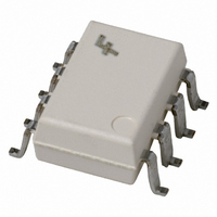
FOD2743BSV Fairchild Optoelectronics Group, FOD2743BSV Datasheet - Page 4

FOD2743BSV
Manufacturer Part Number
FOD2743BSV
Description
OPTOISOLATOR ERROR AMP 8-SMD
Manufacturer
Fairchild Optoelectronics Group
Datasheet
1.FOD2743BSDV.pdf
(16 pages)
Specifications of FOD2743BSV
Number Of Channels
1
Input Type
DC
Voltage - Isolation
5000Vrms
Current Transfer Ratio (min)
50% @ 1mA
Current Transfer Ratio (max)
100% @ 1mA
Voltage - Output
70V
Current - Output / Channel
50mA
Vce Saturation (max)
400mV
Output Type
Transistor
Mounting Type
Surface Mount
Package / Case
8-SMD
Lead Free Status / RoHS Status
Lead free / RoHS Compliant
Current - Dc Forward (if)
-
Other names
FOD2743BSVFS
FOD2743BSVFS
FOD2743BSV_NL
FOD2743BSV_NL
FOD2743BSVFS
FOD2743BSV_NL
FOD2743BSV_NL
©2004 Fairchild Semiconductor Corporation
FOD2743A, FOD2743B, FOD2743C Rev. 1.0.1
Electrical Characteristics
Input Characteristics
Output Characteristics
Transfer Characteristics
Notes:
2. The deviation parameters V
3. The dynamic impedance is defined as |Z
V
Symbol
V
I
REF (DEV)
where T
Symbol
Z
Symbol
REF (DEV)
CE (SAT)
I
minimum values obtained over the rated temperature range. The average full-range temperature coefficient of the
reference input voltage, V
resistors (see Figure 2), the total dynamic impedance of the circuit is given by:
LED (MIN)
CTR
BV
BV
OUT, TOT
V
|Z
V
I
V
I
V
I
(OFF)
CEO
REF
REF
V
COMP
OUT
REF
REF
ECO
CEO
F
|
/
(2)
ppm/°C
(2)
A
Parameter
Current Transfer Ratio
Collector-Emitter Saturation
Voltage
=
is the rated operating free-air temperature range of the device.
Collector Dark Current
Emitter-Collector Voltage Breakdown
Collector-Emitter Voltage Breakdown
LED Forward Voltage
Reference Voltage
Deviation of V
Temperature
Ratio of V
to the Output of the
Error Amplifier
Feedback Input Current I
Deviation of I
Temperature
Minimum Drive Current V
Off-State Error
Amplifier Current
Error Amplifier Output
Impedance
------- -
V
I
Parameter
=
Z
OUT
---------------------------------------------------------------------------------------------------- -
REF
V
(3)
REF DEV
(2)
REF
Parameter
REF
Variation
REF
REF(DEV)
1
Over
Over
+
, is defined as:
R1
------- -
R2
/V
(T
REF
A
I
I
T
I
T
V
V
f
LED
LED
LED
LED
and I
A
A
COMP
LED
COMP
= 25°C unless otherwise specified)
T
= -25°C to +85°C
= -25°C to +85°C
1.0 kHz
T
A
= 1mA, V
= 1mA, V
= 1mA
= 1mA, R
OUT
A
= 37V, V
REF(DEV)
I
V
I
I
=
LED
LED
C
= V
= V
CE
Test Conditions
| = V
25°C
= 0.1mA (Fig. 6)
FB
REF
= 5V (Fig. 6)
= 1mA, V
= 1mA, V
Test Conditions
(Fig.1)
FB
COMP
COMP
, I
1
V
V
COMP
= 10k
LED
are defined as the differences between the maximum and
COMP
COMP
= 0 (Fig. 4)
V
I
I
E
C
CE
= 100µA
= 1.0mA
10
Test Conditions
= V
= V
= 1mA to 20mA,
4
/ I
COMP
COMP
= 10V (Fig. 5)
= 10V to V
= 36V to 10V
6
FB
FB
(Fig. 3)
LED
(Fig.1)
. When the device is operating with two external
= V
= V
FB
FB,
REF
,
FOD2743A 2.482 2.495 2.508
FOD2743B 2.470 2.495 2.520
FOD2743C 2.450 2.500 2.550
Device
Min.
All
All
All
All
All
All
All
All
50
Min.
70
7
Min. Typ. Max. Unit
Typ.
Typ.
100
10
1
0.001
1.07
0.45
0.15
-0.4
-0.3
4.5
2
1
Max.
100
0.4
Max.
50
-2.7
-2.0
www.fairchildsemi.com
1.2
1.2
1.0
1.0
0.5
17
4
Unit
Unit
mV/V
%
nA
V
mV
mA
V
V
µA
µA
µA
V
V
V
V


