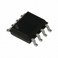
FOD2712 Fairchild Optoelectronics Group, FOD2712 Datasheet - Page 11

FOD2712
Manufacturer Part Number
FOD2712
Description
OPTOISOLATOR ERROR AMP 8SOIC
Manufacturer
Fairchild Optoelectronics Group
Datasheet
1.FOD2712R1V.pdf
(15 pages)
Specifications of FOD2712
Number Of Channels
1
Input Type
DC
Voltage - Isolation
2500Vrms
Current Transfer Ratio (min)
100% @ 10mA
Current Transfer Ratio (max)
200% @ 10mA
Voltage - Output
30V
Current - Output / Channel
50mA
Vce Saturation (max)
400mV
Output Type
Transistor
Mounting Type
Surface Mount
Package / Case
8-SOIC
Lead Free Status / RoHS Status
Lead free / RoHS Compliant
Current - Dc Forward (if)
-
Other names
FOD2712FS
FOD2712FS
FOD2712_NL
FOD2712_NL
FOD2712FS
FOD2712_NL
FOD2712_NL
Available stocks
Company
Part Number
Manufacturer
Quantity
Price
Part Number:
FOD2712
Manufacturer:
FAIRCHILD/仙童
Quantity:
20 000
Part Number:
FOD2712AR2
Manufacturer:
FAIRCHILD/仙童
Quantity:
20 000
Company:
Part Number:
FOD2712R2
Manufacturer:
FSC
Quantity:
5 000
Company:
Part Number:
FOD2712R2
Manufacturer:
JPC
Quantity:
5 000
Part Number:
FOD2712R2
Manufacturer:
FAIRCHILD/仙童
Quantity:
20 000
©2003 Fairchild Semiconductor Corporation
FOD2712 Rev. 1.0.0
The FOD2712
The FOD2712 is an optically isolated error amplifier. It
incorporates three of the most common elements neces-
sary to make an isolated power supply, a reference volt-
age, an error amplifier, and an optocoupler. It is
functionally equivalent to the popular RC431A shunt
voltage regulator plus the CNY17F-3 optocoupler.
Powering the Secondary Side
The LED pin in the FOD2712 powers the secondary
side, and in particular provides the current to run the
LED. The actual structure of the FOD2712 dictates the
minimum voltage that can be applied to the LED pin: The
error amplifier output has a minimum of the reference
voltage, and the LED is in series with that. Minimum volt-
age applied to the LED pin is thus 1.24V + 1.5V = 2.74V.
This voltage can be generated either directly from the
output of the converter, or else from a slaved secondary
winding. The secondary winding will not affect regula-
tion, as the input to the FB pin may still be taken from the
output winding.
The LED pin needs to be fed through a current limiting
resistor. The value of the resistor sets the amount of
current through the LED, and thus must be carefully
selected in conjunction with the selection of the primary
side resistor.
Feedback
Output voltage of a converter is determined by selecting
a resistor divider from the regulated output to the FB pin.
The FOD2712 attempts to regulate its FB pin to the ref-
erence voltage, 1.24V. The ratio of the two resistors
should thus be:
The absolute value of the top resistor is set by the input
offset current of 0.8µA. To achieve 1% accuracy, the
resistance of R
------------------------- -
R
V
------------------------------- -
BOTTOM
R
OUT
R
TOP
TOP
–
1.24
TOP
=
>
V
-------------- 1
V
should be:
OUT
REF
80 A
–
11
Compensation
The compensation pin of the FOD2712 provides the
opportunity for the designer to design the frequency
response of the converter. A compensation network may
be placed between the COMP pin and the FB pin. In typ-
ical low-bandwidth systems, a 0.1µF capacitor may be
used. For converters with more stringent requirements, a
network should be designed based on measurements of
the system’s loop. An excellent reference for this pro-
cess may be found in “Practical Design of Power
Supplies” by Ron Lenk, IEEE Press, 1998.
Secondary Ground
The GND pin should be connected to the secondary
ground of the converter.
No Connect Pins
The NC pins have no internal connection. They should
not have any connection to the secondary side, as this
may compromise the isolation structure.
Photo-Transistor
The Photo-transistor is the output of the FOD2712. In a
normal configuration the collector will be attached to a
pull-up resistor and the emitter grounded. There is no
base connection necessary.
The value of the pull-up resistor, and the current limiting
resistor feeding the LED, must be carefully selected to
account for voltage range accepted by the PWM IC, and
for the variation in current transfer ratio (CTR) of the
opto-isolator itself.
Example: The voltage feeding the LED pins is +12V, the
voltage feeding the collector pull-up is +10V, and the
PWM IC is the Fairchild KA1H0680, which has a 5V ref-
erence. If we select a 10K
maximum current the LED can see is:
(12V–2.74V) /10K = 926µA.
The CTR of the opto-isolator is a minimum of 100%, and
so the minimum collector current of the photo-transistor
when the diode is full on is also 926µA. The collector
resistor must thus be such that:
select 10K to allow some margin.
-----------------------------------
R
COLLECTOR
10V 5V
–
<
926 A or R
COLLECTOR
resistor for the LED, the
>
www.fairchildsemi.com
5.4K ;


