DS1921Z-F5# Maxim Integrated Products, DS1921Z-F5# Datasheet - Page 8
DS1921Z-F5#
Manufacturer Part Number
DS1921Z-F5#
Description
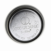
IBUTTON THERMOCHRON F5
Manufacturer
Maxim Integrated Products
Series
iButton®r
Specifications of DS1921Z-F5#
Rohs Information
IButton RoHS Compliance Plan
Memory Size
512B
Memory Type
NVSRAM (Non-Volatile SRAM)
Lead Free Status / RoHS Status
Lead free / RoHS Compliant


Thermochron iButton
histogram memory; and 2048 bytes of data-logging
memory. Except for the ROM and the scratchpad, all
other memory is arranged in a single linear address
space. All memory reserved for logging purposes,
including counter registers and several other regis-
ters, is read-only for the user. The timekeeping and
control registers are write protected while the device
is programmed for a mission.
The hierarchical structure of the 1-Wire protocol is
shown in Figure 2. The bus master must first provide
one of the seven ROM function commands: Read ROM,
Match ROM, Search ROM, Conditional Search ROM,
Skip ROM, Overdrive-Skip ROM, or Overdrive-Match
ROM. Upon completion of an Overdrive ROM com-
mand byte executed at standard speed, the device
enters overdrive mode, where all subsequent communi-
cation occurs at a higher speed. The protocol required
for these ROM function commands is described in
Figure 13. After a ROM function command is success-
fully executed, the memory functions become accessi-
ble and the master can provide any one of the seven
Figure 2. Hierarchical Structure for 1-Wire Protocol
8
_______________________________________________________________________________________
MASTER
BUS
FUNCTION COMMANDS
FUNCTION COMMANDS
COMMAND LEVEL:
MEMORY/CONTROL
DS1921G-SPECIFIC
1-Wire ROM
1-Wire NET
AVAILABLE COMMANDS:
READ ROM
MATCH ROM
SEARCH ROM
SKIP ROM
OVERDRIVE-SKIP ROM
OVERDRIVE-MATCH ROM
CONDITIONAL SEARCH ROM
WRITE SCRATCHPAD
READ SCRATCHPAD
COPY SCRATCHPAD
READ MEMORY
READ MEMORY WTH CRC
CLEAR MEMORY
CONVERT TEMPERATURE
OTHER DEVICES
COMMAND CODES:
available commands. The protocol for these memory
function commands is described in Figure 10. All data
is read and written least significant bit first.
Figure 1 shows the parasite-powered circuitry. This cir-
cuitry “steals” power whenever the IO input is high. IO
provides sufficient power as long as the specified tim-
ing and voltage requirements are met. The advantages
of parasite power are two-fold: 1) By parasiting off this
input, battery power is not consumed for 1-Wire ROM
function commands, and 2) if the battery is exhausted
for any reason, the ROM may still be read normally. The
remaining circuitry of the DS1921G is solely operated
by battery energy.
Each DS1921G contains a unique ROM code that is 64
bits long. The first 8 bits are a 1-Wire family code. The
next 48 bits are a unique serial number. The last 8 bits
are a cyclic redundancy check (CRC) of the first 56 bits
(see Figure 3 for details). The 1-Wire CRC is generated
DS1921G
33h
55h
F0h
CCh
3Ch
69h
ECh
0Fh
AAh
55h
F0h
A5h
3Ch
44h
DATA FIELD AFFECTED:
64-BIT ROM
64-BIT ROM
64-BIT ROM
N/A
OD-FLAG
64-BIT ROM, OD-FLAG
64-BIT ROM, CONDITIONAL SEARCH
256-BIT SCRATCHPAD, FLAGS
256-BIT SCRATCHPAD
4096-BIT SRAM, REGISTERS, FLAGS
ALL MEMORY
ALL MEMORY
MISSION TIMESTAMP, MISSION SAMPLES COUNTER,
MEMORY ADDRESS 211h
SETTINGS, DEVICE STATUS
START DELAY, SAMPLE RATE, ALARM TIMESTAMPS
AND DURATIONS, HISTOGRAM MEMORY
64-Bit Lasered ROM
Parasite Power
Related parts for DS1921Z-F5#
Image
Part Number
Description
Manufacturer
Datasheet
Request
R

Part Number:
Description:
MAX7528KCWPMaxim Integrated Products [CMOS Dual 8-Bit Buffered Multiplying DACs]
Manufacturer:
Maxim Integrated Products
Datasheet:
Part Number:
Description:
Single +5V, fully integrated, 1.25Gbps laser diode driver.
Manufacturer:
Maxim Integrated Products
Datasheet:
Part Number:
Description:
Single +5V, fully integrated, 155Mbps laser diode driver.
Manufacturer:
Maxim Integrated Products
Datasheet:
Part Number:
Description:
VRD11/VRD10, K8 Rev F 2/3/4-Phase PWM Controllers with Integrated Dual MOSFET Drivers
Manufacturer:
Maxim Integrated Products
Datasheet:
Part Number:
Description:
Highly Integrated Level 2 SMBus Battery Chargers
Manufacturer:
Maxim Integrated Products
Datasheet:
Part Number:
Description:
Current Monitor and Accumulator with Integrated Sense Resistor; ; Temperature Range: -40°C to +85°C
Manufacturer:
Maxim Integrated Products
Part Number:
Description:
TSSOP 14/A�/RS-485 Transceivers with Integrated 100O/120O Termination Resis
Manufacturer:
Maxim Integrated Products
Part Number:
Description:
TSSOP 14/A�/RS-485 Transceivers with Integrated 100O/120O Termination Resis
Manufacturer:
Maxim Integrated Products
Part Number:
Description:
QFN 16/A�/AC-DC and DC-DC Peak-Current-Mode Converters with Integrated Step
Manufacturer:
Maxim Integrated Products
Part Number:
Description:
TDFN/A/65V, 1A, 600KHZ, SYNCHRONOUS STEP-DOWN REGULATOR WITH INTEGRATED SWI
Manufacturer:
Maxim Integrated Products
Part Number:
Description:
Integrated Temperature Controller f
Manufacturer:
Maxim Integrated Products
Part Number:
Description:
SOT23-6/I�/45MHz to 650MHz, Integrated IF VCOs with Differential Output
Manufacturer:
Maxim Integrated Products
Part Number:
Description:
SOT23-6/I�/45MHz to 650MHz, Integrated IF VCOs with Differential Output
Manufacturer:
Maxim Integrated Products
Part Number:
Description:
EVALUATION KIT/2.4GHZ TO 2.5GHZ 802.11G/B RF TRANSCEIVER WITH INTEGRATED PA
Manufacturer:
Maxim Integrated Products
Part Number:
Description:
QFN/E/DUAL PCIE/SATA HIGH SPEED SWITCH WITH INTEGRATED BIAS RESISTOR
Manufacturer:
Maxim Integrated Products
Datasheet: