SDCFCF-001G-388 SanDisk, SDCFCF-001G-388 Datasheet - Page 5
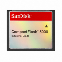
SDCFCF-001G-388
Manufacturer Part Number
SDCFCF-001G-388
Description
COMPACT FLASH IND 1GB FIXED
Manufacturer
SanDisk
Type
CompactFlashr
Datasheet
1.SDCFCF-001G-388.pdf
(97 pages)
Specifications of SDCFCF-001G-388
Memory Size
1GB
Memory Type
CompactFLASH
Density
1GByte
Operating Supply Voltage (typ)
3.3/5V
Operating Temperature (min)
0C
Operating Temperature (max)
70C
Package Type
Not Required
Mounting
Desktop
Pin Count
50
Operating Temperature Classification
Commercial
Operating Supply Voltage (min)
3.135/4.5V
Operating Supply Voltage (max)
3.465/5.5V
Programmable
Yes
Lead Free Status / RoHS Status
Lead free / RoHS Compliant


SanDisk Industrial Grade CompactFlash 5000
Product Manual
List of Tables
Table 1: Formatted Capacities............................................................................................... 7
Table 2: Environmental Specifications.................................................................................. 7
Table 3: Power Requirements: .............................................................................................. 8
Table 4: Performance: ........................................................................................................... 8
Table 5: Reliability: ............................................................................................................... 9
Table 6: Dimensions.............................................................................................................. 9
Table 7: PC Card Memory Mode Pin Assignments ............................................................ 11
Table 8: PC Card I/O Mode Pin Assignments..................................................................... 12
Table 9: True IDE Mode Pin Assignments ......................................................................... 13
Table 10: Signal Description ............................................................................................... 14
Table 11: Input Leakage Control......................................................................................... 17
Table 12: Input Characteristics............................................................................................ 17
Table 13: Output Drive Type............................................................................................... 18
Table 14: Output Drive Characteristics ............................................................................... 18
Table 15: Power Up/Power Down Timing .......................................................................... 19
Table 16: Common Memory Read Timing Specification ................................................... 20
Table 17: Common and Attribute Memory Write Timing Specification ........................... 21
Table 18: Attribute Memory Read Timing Specification.................................................... 22
Table 19: I/O Read (Input) Timing Specification ............................................................... 24
Table 20: I/O Write Timing Specification........................................................................... 25
Table 21: Register Transfer to/from Device........................................................................ 26
Table 22: PIO Data Transfer to/from Device ...................................................................... 27
Table 23: Registers and Memory Space Decoding ............................................................. 28
Table 24: Configuration Registers Decoding ...................................................................... 29
Table 25: Attribute Memory Function ................................................................................ 30
Table 26: Card Configurations ............................................................................................ 31
Table 27: Pin Replacement Changed Bit/Mask Bit Values................................................. 32
Table 28: Common Memory Function ................................................................................ 33
Table 29: IDE Mode I/O Function ...................................................................................... 34
Table 30: Standard I/O Configurations ............................................................................... 35
Table 31: Primary and Secondary I/O Decoding................................................................. 35
Table 32: Contiguous I/O Decoding.................................................................................... 36
Table 33: Memory Mapped Decoding ................................................................................ 37
Table 34: True IDE Mode I/O Decoding ............................................................................ 38
© 2007 SanDisk® Corporation
iv
April 2007
Related parts for SDCFCF-001G-388
Image
Part Number
Description
Manufacturer
Datasheet
Request
R

Part Number:
Description:
COMPACT FLASH IND 512MB FIXED
Manufacturer:
SanDisk
Datasheet:
Part Number:
Description:
COMPACT FLASH IND 2GB FIXED
Manufacturer:
SanDisk
Datasheet:
Part Number:
Description:
COMPACT FLASH IND 4GB FIXED
Manufacturer:
SanDisk
Datasheet:
Part Number:
Description:
COMPACT FLASH IND 8GB FIXED
Manufacturer:
SanDisk
Datasheet:

Part Number:
Description:
IC MDOC G4 2GB 69-FBGA
Manufacturer:
SanDisk
Datasheet:
Part Number:
Description:
IC MDOC P3 256MB 48-TSOP
Manufacturer:
SanDisk
Datasheet:
Part Number:
Description:
IC MDOC P3 256MB 48-TSOP
Manufacturer:
SanDisk
Datasheet:
Part Number:
Description:
IC MDOC P3 256MB 48-TSOP
Manufacturer:
SanDisk
Datasheet:
Part Number:
Description:
IC MDOC H1 8GB 115-FBGA
Manufacturer:
SanDisk
Datasheet:
Part Number:
Description:
IC MDOC H3 1GB FBGA
Manufacturer:
SanDisk
Datasheet: