SDCFIR-002G-388 SanDisk, SDCFIR-002G-388 Datasheet - Page 21
SDCFIR-002G-388
Manufacturer Part Number
SDCFIR-002G-388
Description
COMPACT FLASH IND 2GB
Manufacturer
SanDisk
Datasheet
1.SDCFCF-001G-388.pdf
(97 pages)
Specifications of SDCFIR-002G-388
Memory Size
2GB
Memory Type
CompactFLASH
Lead Free Status / RoHS Status
Lead free / RoHS Compliant
Other names
585-1235
SDCFIR-002G-388
SDCFIR-002G-388


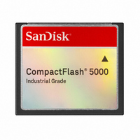
SanDisk Industrial Grade CompactFlash 5000
A10-A0 (PC Card Memory
Mode) (PC Card I/O Mode)
A2-A0 (True IDE Mode) A10-
A3 (True IDE Mode)
BVD1 (PC Card Memory
Mode) -STSCHG (PC Card
I/O Mode) -PDIAG (True IDE
Mode)
BVD2 (PC Card Memory
Mode) -SPKR (PC Card I/O
Mode) -DASP (True IDE
Mode)
-CD1, -CD2 (PC Card Memory
Mode) (PC Card I/O Mode)
(True IDE Mode)
-CE1, -CE2 (PC Card Memory
Mode) (PC Card I/O Mode) -
CS0, -CS1 (True IDE Mode)
-CSEL (PC Card Memory
Mode) (PC Card I/O Mode)
-CSEL (True IDE Mode)
D15-D00 (PC Card Memory
Mode) (PC Card I/O Mode)
D15-D00 (True IDE Mode)
GND (PC Card Memory
Mode) (PC Card I/O Mode)
© 2007 SanDisk® Corporation
Signal Name
I/O
Dir.
I/O
I/O
I I
O
I
I
14, 15, 16, 17,
31, 30, 29, 28,
27, 49, 48, 47,
18, 19, 20 18,
8, 10, 11, 12,
6, 5, 4, 3, 2,
23, 22, 21
19, 20
26, 25
7, 32
1, 50
Pin
46
45
39
These address lines, along with the -REG signal, are used to select the following: I/O and memory-mapped
port address registers within the card, a byte in the card's information structure and its configuration control and
status registers. In True IDE Mode only A[2:0] is used to select one of eight registers in the Task File. In True
IDE Mode these remaining address lines should be grounded by the host.
This signal is asserted high as the BVD1 signal since a battery is not used with this product. The Status
Changed signal is asserted low to alert the host to changes in the RDY/-BSY and Write Protect states, while
the I/O interface is configured. Its use is controlled by the Card Config. and Status Register. In True IDE Mode,
this input/output is the Pass Diagnostic signal in the master/slave handshake protocol.
This output line is always driven to a high state in Memory Mode since a battery is not required for this product,
as well as in I/O Mode, since this product does not support the audio function. In True IDE Mode, this
input/output is the Disk Active/Slave Present signal in the master/ slave handshake protocol.
These Card Detect pins are connected to ground on the card. The host uses these pins to determine if the card
is fully inserted into its socket.
The Card Enable input signals are used both to select the card and to indicate to the card whether a byte or a
word operation is being performed. -CE2 always accesses the odd byte of the word. -CE1 accesses either the
even or the odd byte of the word, depending on A0 and -CE2. A multiplexing scheme based on A0, -CE1, -CE2
allows 8 bit hosts to access all data on D0-D7. In True IDE Mode, -CS0 is the chip select for the Task File
registers, while -CS1 is used to select the Alternate Status Register and the Device Control Register.
This signal is not used for PC Card Memory Mode or PC Card I/O Mode.
This internally pulled up signal is used to configure the device as a master or slave when configured in True
IDE Mode. When this pin is grounded, the device is configured as a master. When the pin is open, this device
is configured as a slave.
These lines carry the data, commands and status information between the host and the controller. D00 is the
LSB of the word’s even byte; D08 is the LSB of the word’s odd byte. In True IDE Mode, all Task File operations
occur in byte mode on the low order bus D00D07 while all data transfers are 16 bits using D00-D15.
Ground.
Table 10: Signal Description
14
Description
Product Manual
March 2007
Related parts for SDCFIR-002G-388
Image
Part Number
Description
Manufacturer
Datasheet
Request
R

Part Number:
Description:
COMPACT FLASH IND 1GB
Manufacturer:
SanDisk
Datasheet:
Part Number:
Description:
COMPACT FLASH IND 512MB
Manufacturer:
SanDisk
Datasheet:
Part Number:
Description:
COMPACT FLASH IND 4GB
Manufacturer:
SanDisk
Datasheet:
Part Number:
Description:
COMPACT FLASH IND 8GB
Manufacturer:
SanDisk
Datasheet:

Part Number:
Description:
IC MDOC G4 2GB 69-FBGA
Manufacturer:
SanDisk
Datasheet:
Part Number:
Description:
IC MDOC P3 256MB 48-TSOP
Manufacturer:
SanDisk
Datasheet:
Part Number:
Description:
IC MDOC P3 256MB 48-TSOP
Manufacturer:
SanDisk
Datasheet:
Part Number:
Description:
IC MDOC P3 256MB 48-TSOP
Manufacturer:
SanDisk
Datasheet:
Part Number:
Description:
IC MDOC H1 8GB 115-FBGA
Manufacturer:
SanDisk
Datasheet:
Part Number:
Description:
IC MDOC H3 1GB FBGA
Manufacturer:
SanDisk
Datasheet: