4162135-XX Digital View Inc, 4162135-XX Datasheet
4162135-XX
Manufacturer Part Number
4162135-XX
Description
ADD ON BOARD FOR LVDS DISPLAYS
Manufacturer
Digital View Inc
Datasheet
1.4162135-XX.pdf
(2 pages)
Specifications of 4162135-XX
Accessory Type
Display - LVDS Interface Add-On Board
For Use With/related Products
TFT Panels
Lead Free Status / RoHS Status
Contains lead / RoHS non-compliant
Other names
586-1002


JP3 – Enable DE signal on signal or dual LVDS transmitter chip at even pixel side
Jumper Settings :
JP1- Clock phase selection (Default 2-3 closed)
JP2 - Panel voltage selection
1-3, 2-4 closed : 12V panel
3-5, 4-6 closed : 3.3 / 5V panel (Default)
1-2 closed : Enable DE signal on both LVDS transmitter chips (U1 & U2) (Default - Use for all panels)
2-3 closed : Enable DE signal on single LVDS transmitter chip (U1)
Compatible with LVDS board :
Use of connectors :
The LVDS add-on board P/N 4162135-11 design for dual pixel LVDS panels. It
provides jumper setting to select the Data Enable (DE) signal on transmitter chips.
Old LVDS board
P/N 4162135-10
P/N 4162147-00
Change this setting to obtain best quality.
Connector
CN2
CN3
CN4
CN5
CN6
(Use for all panel except : NEC NL128102AC28-04 and NEC NL128102AC31-02A)
JP1 : 2-3 closed ; JP2 : 1-3, 2-4 closed ; JP3 : 1-2 closed
JP1 : 2-3 closed ; JP2 : 3-5, 4-6 closed ; JP3 : 1-2 closed
Hirose DF11-28DS-2DSA
Hirose DF11-32DS-2DSA
Hirose DF11-20DF-2DSA
Hirose DF14-20P-1.25P
Hirose DF14-25P-1.25P
Jumper setting on LVDS board P/N 4162135-11
Connector type
Page 1 of 2
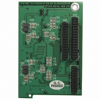
LVDS Add On Board P/N 4162135-11
Related parts for 4162135-XX
Image
Part Number
Description
Manufacturer
Datasheet
Request
R

Part Number:
Description:
POST BIND STRIP 4"L F-GLASS
Manufacturer:
Keystone Electronics
Datasheet:

Part Number:
Description:
KIT OSD BRD W CBL DIGITAL POT
Manufacturer:
Digital View Inc
Datasheet:

Part Number:
Description:
Display Modules & Development Tools OSD DIGITAL I/F BRD 300MM CABLE
Manufacturer:
Digital View Inc
Datasheet:
Part Number:
Description:
Display Modules & Development Tools Digital OSD Kit
Manufacturer:
Digital View Inc
Datasheet:
Part Number:
Description:
Audio DSPs M3-310 Player w/LVDS & TTL Output
Manufacturer:
Digital View Inc

Part Number:
Description:
Audio DSPs M3-310 Player w/LVDS & TTL Output
Manufacturer:
Digital View Inc

Part Number:
Description:
BOARD PC/DVI INTERFACE ALR-1400
Manufacturer:
Digital View Inc

Part Number:
Description:
CTLR DVI-2560 DUAL LINK DVI 24V
Manufacturer:
Digital View Inc
4162135-XX Summary of contents
Page 1
... The LVDS add-on board P/N 4162135-11 design for dual pixel LVDS panels. It provides jumper setting to select the Data Enable (DE) signal on transmitter chips. Jumper Settings : JP1- Clock phase selection (Default 2-3 closed) Change this setting to obtain best quality. JP2 - Panel voltage selection 1-3, 2-4 closed : 12V panel 3-5, 4-6 closed : 3 ...
Page 2
Mechanical Drawing : Pin Assignments : CN5 - Hirose DF14-20P-1.25P PIN SYMBOL DESCRIPTION connection 2 GND 3 OUTO3 Positive differential LVDS data O3 4 /OUTO3 Negative differential LVDS data O3 5 GND 6 CLKOUTO Positive LVDS clock ...