T-51638D084-FW-A-AA Optrex America Inc, T-51638D084-FW-A-AA Datasheet
T-51638D084-FW-A-AA
Specifications of T-51638D084-FW-A-AA


Related parts for T-51638D084-FW-A-AA


T-51638D084-FW-A-AA Summary of contents
Page 1
... INSPECTION STANDARDS 11 HANDLING PRECAUTIONS FOR TFT-LCD MODULE -- PACKAGING SPECIFICATION -- PRODUCT NUMBER LABELING FORMS -- LAMP UNIT FOR 8.4 VGA T-51638D084-FW-A-AA (AA) No. 2002-0213 Approved by Checked by (Quality Assurance Division) Checked by (ACI Engineering Division) Prepared by (Production Engineering Group) Item OPTREX CORPORATION First Edition Oct 10, 2002 ...
Page 2
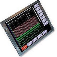
... OVERVIEW T-51638D084-FW-A-AA is 8.4” color TFT-LCD (Thin Film Transistor Liquid Crystal Display) module composed of LCD panel, driver ICs, control circuit, and backlight unit. By applying 6 bit digital data, 640 screen. Input power voltage is single 3.3V for LCD driving. Inverter for backlight is not included in this module. General specifications are summarized in ...
Page 3
... Permissive input ripple Voltage Logic Input Voltage (2) Backlight ITEM Lamp Voltage Lamp Current Lamp Frequency Starting Lamp Voltage Lamp Life Time *1) Lamp Current measurement method (The current meter is inserted in low voltage line.) LCD Module T-51638D084-FW-A-AA (AA) No. 2002-0213 SYMBOL VCC stg SYMBOL MIN ...
Page 4
... VCC-dip conditions: 1) When 2.6 V VCC < 3 When VCC < 2.6 V VCC-dip conditions should also follow the power and signals sequence. B) Typical current condition: 64- gray- bar-pattern 480 line mode VCC = +3 Normal value, not peak value T-51638D084-FW-A-AA (AA) No. 2002-0213 400 200 VCC 3.0 V data 0.5 V ...
Page 5
... Reverse scan control Normal Reverse *) The shielding case is connected with GND (BACKLIGHT) Backlight-side connector: BHR-02(8.0)VS-1N(JST) Inverter-side connector: SM02(8.0)B-BHS(JST) Pin No [Note]VBLH-VBLL = VL T-51638D084-FW-A-AA (AA) No. 2002-0213 Function Symbol Function CTH VBLH(High Voltage) CTL VBLL(Low Voltage) OPTREX CORPORATION Page 5/32 ...
Page 6
... DATA is latched at fall edge of DCLK in this timing specification. *2) Polarities of HD and VD are negative in this specification. *3) DENA (Data Enable) should always be positive polarity as shown in the timing specification. *4) DCLK should appear during all invalid period, and HD should appear during invalid period of frame cycle. T-51638D084-FW-A-AA (AA) No. 2002-0213 SYMBOL MIN. TYP. f ...
Page 7
... Pixel Timing Chart DCLK DATA(R,G,B), DENA, HD Horizontal Timing Chart DCLK DATA Invalid Data (R,G, HFP DENA t WHL HD c. Vertical Timing Chart HD LINE DATA t VFP DENA VD T-51638D084-FW-A-AA (AA) No. 2002-0213 t CLK t t WCH WCL 2.0V 0. DS DH 2.0V 0.8V First Data HBP HA t ...
Page 8
... BASIC BLUE(63) 0 COLOR CYAN 0 MAGENTA 1 YELLOW 1 WHITE 1 RED(0) 0 RED (1) 0 RED(2) 0 RED RED (62) 1 RED(63) 1 GREEN(0) 0 GREEN (1) 0 GREEN(2) 0 GREEN GREEN(62) 0 GREEN(63) 0 BLUE(0) 0 BLUE(1) 0 BLUE(2) 0 BLUE BLUE(62) 0 BLUE(63) 0 [Note]1) Definition of gray scale Color (n) --- Higher n means brighter level. T-51638D084-FW-A-AA (AA) No. 2002-0213 R DATA LSB ...
Page 9
... Data 1:High, 0: Low T-51638D084-FW-A-AA (AA) No. 2002-0213 OPTREX CORPORATION Page 9/32 ...
Page 10
... BLOCK DIAGLAM Timing signal Display data Timing Converter Power Power Supply Circuit BACKLIGHT T-51638D084-FW-A-AA (AA) No. 2002-0213 CN2,CN3 CCFL 1 3 OPTREX CORPORATION BACKLIGHT Driver(source TFT-LCD G480 BACKLIGHT CN2 CN3 Page 10/32 ...
Page 11
... MECHANICAL SPECIFICATIONS (1) Front Side T-51638D084-FW-A-AA (AA) No. 2002-0213 Tolerance is ±0.5mm unless noted. OPTREX CORPORATION Page 11/32 ...
Page 12
... Rear Side [Note] We recommend you referring to the detailed drawing for your design. Please contact our company sales representative when you need the detailed drawing. T-51638D084-FW-A-AA (AA) No. 2002-0213 Tolerance is ±0.5mm unless noted. OPTREX CORPORATION Page 12/32 ...
Page 13
... CR=ON (White) Luminance / OFF(Black) Luminance: average of 5 points shown in a figure below *2) Definition of Luminance Lw= ON (White) Luminance: average of 5 points shown in a figure below (1,1) 120 240 360 T-51638D084-FW-A-AA (AA) No. 2002-0213 Ta = 25°C, VCC = 3.3 V, Input Signals: Typ. Values shown in Section 5 MIN ...
Page 14
... Definition of Viewing Angle ( *4) Definition of Response Time Luminance *5) Image Sticking Continuously display the test pattern shown in the figure below for two-hours. Then display a completely white screen. The previous image shall not persist more than two seconds at 25°C. T-51638D084-FW-A-AA (AA) No. 2002-0213 ) White 90% 10% tr ...
Page 15
... The judgment of the above tests should be made as follow: Pass: Normal display image with no obvious non-uniformity and no line defect. Partial transformation of the module parts should be ignored. Fail: No display image, obvious non-uniformity, or line defects. T-51638D084-FW-A-AA (AA) No. 2002-0213 40°C, 90%RH, 240 h BETWEEN -20°C (1h) and 65°C(1h), CONDITIONS ...