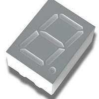
HDSP-F401 Avago Technologies US Inc., HDSP-F401 Datasheet - Page 6

HDSP-F401
Manufacturer Part Number
HDSP-F401
Description
DISPLAY 7SEGMENT ORANGE CA
Manufacturer
Avago Technologies US Inc.
Type
Moduler
Specifications of HDSP-F401
Display Type
7-Segment
Common Pin
Common Anode
Number Of Digits/alpha
1
Size / Dimension
0.51" L x 0.39" W x 0.25" H (12.90mm x 9.79mm x 6.36mm)
Digit/alpha Size
0.40" (10.16mm)
Color
Orange
Voltage - Forward (vf) Typ
2V
Current - Test
5mA
Millicandela Rating
1.2mcd
Wavelength - Peak
600nm
Power Dissipation (max)
105mW
Package / Case
10-DIP (0.300", 7.62mm)
Number Of Digits
1
Illumination Color
Orange
Operating Current
5 mA
Luminous Intensity
1200 ucd
Package Type
DIP
Product Length (mm)
12.9mm
Product Height (mm)
6.36mm
Product Depth (mm)
9.79mm
Digit Size (in)
.4in
Character Displayed
Numeric
Viewing Area Length (mm)
5.59mm
Viewing Area Height (mm)
10.16mm
Emitting Color
Orange
Forward Voltage
2.5V
Test Current (it)
5mA
Forward Current
30mA
Dominant Wave Length
603nm
Power Dissipation
105mW
Total Thickness
6.36mm
Reverse Voltage
30V
Mounting
Through Hole
Operating Temperature Classification
Industrial
Pin Count
10
Configuration
Common Anode
Number Of Elements
8
Peak Wavelength
600nm
Lead Free Status / RoHS Status
Lead free / RoHS Compliant
Lead Free Status / RoHS Status
Lead free / RoHS Compliant, Lead free / RoHS Compliant
Electrical/Optical Characteristics at T
High Efficiency Red
Orange
6
Device
Device
Series
HDSP-
Series
HDSP-
F40x/
G40x
F20x/
G20x
Luminous Intensity/Segment
Forward Voltage/Segment or DP
Peak Wavelength
Dominant Wavelength
Reverse Voltage/Segment or DP
Temperature Coefficient of
V
Thermal Resistance LED
Junction-to-Pin
Luminous Intensity/Segment
Forward Voltage/Segment or DP
Peak Wavelength
Dominant Wavelength
Reverse Voltage/Segment or DP
Temperature Coefficient of
V
Thermal Resistance LED
Junction-to-Pin
(Digit Average)
(Digit Average)
F
F
/Segment or DP
/Segment or DP
Parameter
Parameter
[3]
[3]
A
= 25 C, continued
[1,2]
[1,2]
[4]
[4]
Symbol
Symbol
Rl\q
R
V
l
V
PEAK
V
PEAK
V
V
V
I
F
J-PIN
I
l
F
V
V
d
F
d
R
F
R
/ C
J-PIN
/ C
Min.
Min.
420
420
3.0
3.0
1200
1200
Typ.
Typ.
635
626
320
600
603
320
2.0
2.0
30
30
-2
-2
Max.
Max.
2.5
2.5
C/W/Seg
C/W/Seg
mV/ C
mV/ C
Units
Units
nm
nm
nm
nm
V
V
V
V
cd
cd
Test Conditions
I
I
I
Test Conditions
I
I
I
F
F
R
F
F
R
= 5 mA
= 20 mA
= 100 A
= 5 mA
= 20 mA
= 100 A


