HCMS-3904 Avago Technologies US Inc., HCMS-3904 Datasheet
HCMS-3904
Specifications of HCMS-3904
Available stocks


Related parts for HCMS-3904


HCMS-3904 Summary of contents
Page 1
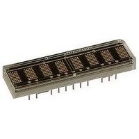
... V High Performance CMOS 5x7 AlphaNumeric Displays Data Sheet HCMS-3901, HCMS-3902, HCMS-3961, HCMS-3962, HCMS-3911, HCMS-3912, HCMS-3971, HCMS-3972 HCMS-3903, HCMS-3904, HCMS-3963, HCMS-3964, HCMS-3913, HCMS-3914, HCMS-3973, HCMS-3974 Description The 3.3 V HCMS-39xx family is similar to the 5.0 V HCMS-29xx family, except it operates at a lower operating voltage. Package dimen sions and pin outs are exactly the same for both families ...
Page 2
... TYP. (0.020 ± 0.005) 2.54 ± 0.13 (0.100 ± 0.005) (NON ACCUM.) Figure 2. HCMS-391X Package dimensions NOTES: 1. DIMENSIONS ARE IN mm (INCHES). 2. UNLESS OTHERWISE SPECIFIED, TOLERANCE ON DIMENSIONS IS ± 0.38 mm (0.015 INCH). 3. LEAD MATERIAL: SOLDER PLATED COPPER ALLOY. 2 PIN FUNCTION ...
Page 3
... PART NUMBER HCMS-397x YYWW 0.51 (0.020) 0.51 ± 0.13 TYP. (0.020 ± 0.005) Figure 4. HCMS-397X Package dimensions NOTES: 1. DIMENSIONS ARE IN mm (INCHES). 2. UNLESS OTHERWISE SPECIFIED, TOLERANCE ON DIMENSIONS IS ± 0.38 mm (0.015 INCH). 3. LEAD MATERIAL: SOLDER PLATED COPPER ALLOY. 3 2.54 (0.100) TYP. 3 11.43 (0.450) MAX. ...
Page 4
... For further description, see Appendix B, Electrical Considerations, “VLOGIC and VLED Considerations”. 4 Red HCMS-3902 HCMS-3912 HCMS-3962 HCMS-3972 ..................................... -0 7.0 V LOGIC ................................................ -0 5 [1] ................................ -40°C to +85°C [1] = 25°C A Min. Max. Units 3.1 5.5 V 3.1 5.5 V -0.3 +0.3 V Green Orange HCMS-3903 HCMS-3904 HCMS-3913 HCMS-3914 HCMS-3963 HCMS-3964 HCMS-3973 HCMS-3974 +0.3 V LOGIC ...
Page 5
... Refers to the initial case temperature of the device immediately prior to measurement. 2. For comparison purpose with existing HCMS-29xx 5 V devices. The Typical and Minimum Luminous Intensity per LED Character Average can be calculated by dividing the values in the table by two for the test condition 50% Peak Current, 100% Pulse Width and V 3. Measured with all LEDs illuminated in a digit. 4. Dominant wavelength, λ ...
Page 6
Electrical Description Pin Function Description RESET (RST) Sets Control Register bits to logic low. The Dot Register contents are unaffected by the Reset pin. (logic low = reset; logic high = normal operation). DATA Serial Data input ...
Page 7
AC Timing Characteristics over Temperature Range (-40 to +85°C) Timing Diagram Ref. Number Description 1 Register Select Setup Time to Chip Enable 2 Register Select Hold Time to Chip Enable 3 Rising Clock Edge to Falling Chip Enable Edge 4 ...
Page 8
... Display Overview The HCMS-39XX series is a family of LED displays driven by on-board CMOS ICs. The LEDs are configured as 5x7 font characters and are driven in groups of 4 characters per IC. Each IC consists of a 160-bit shift register (the Dot Register), two 7-bit Control Words, and refresh circuitry. ...
Page 9
... REGISTERS NOTE: 1. DATA IS COPIED TO THE CONTROL REGISTER OR THE DOT LATCH AND LED OUTPUTS WHEN CE IS HIGH AND CLK IS LOW. Figure 5. HCMS-39XX write cycle timing diagram Pixel Map In a 4-character display, the 160-bits are arranged as 20 columns by 8 rows. This array can be conceptualized as four dot matrix character locations, but only 7 of the 8 rows have LEDs (see Figures 6 & ...
Page 10
... CLR REGISTER D Q SELECT RS (LATCHED) REFRESH CONTROL RESET RST PRESCALE VALUE H ÷8 OSC OSCILLATOR L H OSC SELECT BLANK Figure 6. Block diagram for HCMS-39xx 10 DATA OUT RS (LATCHED SER/PAR MODE DI 40 BIT 40 BIT S.R. DATA DO DO OUT CURRENT REFERENCE ANODE PWM BRIGHTNESS CONTROL 0 ...
Page 11
PIXEL DATA TO NEXT CHARACTER Figure 7. Pixel map 11 DATA FROM PREVIOUS CHARACTER ROW 7 ROW 6 ROW 5 ROW 4 ROW 3 ROW 2 ROW 1 ROW 0 (NOT USED) ...
Page 12
Control Register The Control Register allows software modification of the IC’s operation and consists of two independent 7-bit control words. Bit D in the shift register selects 7 one of the two 7-bit control words. Control Word 0 performs pulse ...
Page 13
Table 2. Control Shift Register. CONTROL WORD Bit D 7 Set Low to Select Control Word 0 Peak Current Brightness Control – DISABLES ...
Page 14
... These bits must always be pro-grammed to logic low. Cascaded ICs is connected OUT Figure 8 shows how two ICs are connected within an HCMS-39XX display. The first IC controls the four left- most characters and the second IC controls the four changes D to OUT right-most characters. The Dot Registers are connected in series to form a 320-bit dot shift register ...
Page 15
RESET CLK RESET CLK D D OUT OUT SEL SEL OSC OSC D IN Figure 8. Cascaded ICs 15 IC1 BITS 0-159 CHARACTERS 0 RESET IC2 BITS 160-319 CLK ...
Page 16
Appendix A. Thermal Considerations The display IC has a maximum junction temperature of 150°C. The IC junction temperature can be calculated with Equation 1 in Table 3. A typical value for Rθ is 100°C/W. This value is typical JA for ...
Page 17
... The inputs to the ICs are protected against static discharge and input current latch up. However, for best results, standard CMOS handling precautions should be used. Before use, the HCMS-39XX should be stored in antistatic tubes or in conductive material. During assembly, a grounded conductive work area should be ...
Page 18
Appendix C. Oscillator The oscillator provides the internal refresh circuitry with a signal that is used to synchronize the columns and rows. This ensures that the right data is in the dot drivers for that row. This signal can be ...