AFBR-5903AZ Avago Technologies US Inc., AFBR-5903AZ Datasheet - Page 7
AFBR-5903AZ
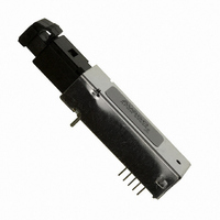
Manufacturer Part Number
AFBR-5903AZ
Description
TXRX OPT FE MTRJ EXT TEMP 2X5DIP
Manufacturer
Avago Technologies US Inc.
Datasheet
1.AFBR-5903AZ.pdf
(16 pages)
Specifications of AFBR-5903AZ
Data Rate
100Mbps
Wavelength
1300nm
Applications
General Purpose
Voltage - Supply
3.3V
Connector Type
MTRJ
Mounting Type
Through Hole
Function
Implement FDDI and ATM at the 100 Mbps/125 MBd rate
Product
Transceiver
Maximum Rise Time
3 ns/2.2 ns
Maximum Fall Time
3 ns/2.2 ns
Pulse Width Distortion
0.12 ns/0.2 ns
Maximum Output Current
50 mA
Operating Supply Voltage
3.135 V to 3.465 V
Maximum Operating Temperature
+ 85 C
Minimum Operating Temperature
- 40 C
Package / Case
DIP With Connector
Lead Free Status / RoHS Status
Lead free / RoHS Compliant
For Use With
Multimode Glass
Lead Free Status / RoHS Status
Lead free / RoHS Compliant, Lead free / RoHS Compliant
Other names
516-1992
Available stocks
Company
Part Number
Manufacturer
Quantity
Price
Company:

Part Number:
AFBR-5903AZ
Manufacturer:
OV
Quantity:
1 000
Company:
Part Number:
AFBR-5903AZ
Manufacturer:
Avago Technologies US Inc.
Quantity:
135


Board Layout - Decoupling Circuit, Ground Planes and
Termination Circuits
It is important to take care in the layout of your circuit board
to achieve optimum performance from these transceivers.
Figure 7 provides a good example of a schematic for a
power supply decoupling circuit that works well with these
parts. It is further recommended that a continuous ground
plane be provided in the circuit board directly under the
transceiver to provide a low inductance ground for signal
return current. This recommendation is in keeping with
good high frequency board layout practices. Figures 7 and
8 show two recommended termination schemes.
Figure 7. Recommended Decoupling and Termination Circuits
7
Note: C1 = C2 = C3 = 10 nF or 100 nF
TX
RX
10
TRANSCEIVER INPUTS
1
TERMINATE AT
9
2
8
3
130 Ω
100
7
4 5
6
130 Ω
C2
C1
Z = 50 Ω
Z = 50 Ω
1 µH
1 µH
V CC (+3.3 V)
C3
Z = 50 Ω
Z = 50 Ω
Z = 50 Ω
10 µF
Board Layout - Hole Pattern
The Avago Technologies transceiver complies with the
circuit board “ Common T ransceiver Footprint” hole pattern
defined in the original multisource announcement which
defined the 2 x 5 package style. T his drawing is reproduced
in Figure 9 with the addition of ANSI Y14.5M compliant
dimensioning to be used as a guide in the mechanical
layout of your circuit board.
130 Ω
TERMINATE AT
DEVICE INPUTS
130 Ω
82 Ω
V CC (+3.3V)
100 Ω
130 Ω
TD-
TD+
RD+
RD-
SD
PHY DEVICE
V CC (+3.3 V)
LVPECL
V CC (+3.3 V)
LVPECL
Related parts for AFBR-5903AZ
Image
Part Number
Description
Manufacturer
Datasheet
Request
R

Part Number:
Description:
650nm FE Transceiver Eval Kit
Manufacturer:
Avago Technologies US Inc.
Datasheet:

Part Number:
Description:
TXRX OPT OC3 MTRJ SFF 2X5DIP
Manufacturer:
Avago Technologies US Inc.
Datasheet:

Part Number:
Description:
TXRX ETHERNET 125MBD MMF 2X5
Manufacturer:
Avago Technologies US Inc.
Datasheet:

Part Number:
Description:
TXRX OPT SFP DGTL 850NM IND
Manufacturer:
Avago Technologies US Inc.
Datasheet:

Part Number:
Description:
TXRX OPT SFF 4/2/1GBD 2X7
Manufacturer:
Avago Technologies US Inc.
Datasheet:

Part Number:
Description:
TXRX OPT SFP 4/2/1GBD 850NM
Manufacturer:
Avago Technologies US Inc.
Datasheet:

Part Number:
Description:
TXRX OPT XFP 10GB/S 850NM
Manufacturer:
Avago Technologies US Inc.
Datasheet:

Part Number:
Description:
TXRX OPT 1X9 100MBPS ST EXT TEMP
Manufacturer:
Avago Technologies US Inc.
Datasheet:

Part Number:
Description:
TXRX OPT 1X9 100MBPS SC EXT TEMP
Manufacturer:
Avago Technologies US Inc.
Datasheet:

Part Number:
Description:
TXRX OPT 1X9 100MBPS DUPLEX SC
Manufacturer:
Avago Technologies US Inc.
Datasheet:

Part Number:
Description:
OPTOCOUPLER GATE DRV 2A 16-SOIC
Manufacturer:
Avago Technologies US Inc.
Datasheet:
Part Number:
Description:
OPTOCOUPLER 2CH 2.5A 16-SOIC
Manufacturer:
Avago Technologies US Inc.
Datasheet:

Part Number:
Description:
OPTOCOUPLER GATE DRV 0.4A 16SOIC
Manufacturer:
Avago Technologies US Inc.
Datasheet:

Part Number:
Description:
OPTOCOUPLER 2.0A 250KHZ 8-DIP
Manufacturer:
Avago Technologies US Inc.
Datasheet:

Part Number:
Description:
OPTOCOUPLER 2.0A 250KHZ GW 8-SMD
Manufacturer:
Avago Technologies US Inc.
Datasheet: