AFCT-5961ATGZ Avago Technologies US Inc., AFCT-5961ATGZ Datasheet - Page 7
AFCT-5961ATGZ
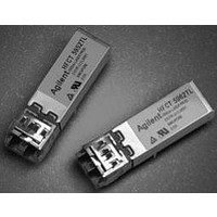
Manufacturer Part Number
AFCT-5961ATGZ
Description
TXRX OPT SM SONET OC3/SDH 2X5
Manufacturer
Avago Technologies US Inc.
Series
METRAKr
Datasheet
1.AFCT-5961TGZ.pdf
(16 pages)
Specifications of AFCT-5961ATGZ
Applications
General Purpose
Data Rate
155Mbps
Wavelength
1300nm
Voltage - Supply
3.1 V ~ 3.5 V
Connector Type
LC Duplex
Mounting Type
Through Hole
Data Rate Max
0.155Gbps
Supply Voltage
3.3V
Wavelength Typ
1300nm
Leaded Process Compatible
Yes
Optical Fiber Type
TX/RX
Data Transfer Rate
155Mbps
Optical Rise Time
2/2.2ns
Optical Fall Time
2/2.2ns
Operating Temperature Classification
Industrial
Peak Wavelength
1360nm
Package Type
DIP With Connector
Operating Supply Voltage (min)
3.1V
Operating Supply Voltage (typ)
3.3V
Operating Supply Voltage (max)
3.5V
Output Current
50mA
Operating Temp Range
-40C to 85C
Mounting
Snap Fit To Panel
Pin Count
10
Lead Free Status / RoHS Status
Lead free / RoHS Compliant
Lead Free Status / RoHS Status
Lead free / RoHS Compliant, Lead free / RoHS Compliant


Application Information
The Applications Engineering Group at Avago Tech-
nologies is available to assist you with technical under-
standing and design trade-offs associated with these
transceivers. You can contact them through your Avago
Technologies sales representative.
The following information is provided to answer some
of the most common questions about the use of the
parts.
Optical Power Budget and
Link Penalties
The worst-case Optical Power Budget (OPB) in dB for a
fiber-optic link is determined by the difference between
the minimum transmitter output optical power (dBm
avg) and the lowest receiver sensitivity (dBm avg). This
OPB provides the necessary optical signal range to
establish a working fiber-optic link. The OPB is allocated
for the fiber-optic cable length and the corresponding
link penalties. For proper link performance, all penalties
that affect the link performance must be accounted for
within the link optical power budget.
Figure 6a. Recommended dc Coupled Interface Circuit
T
7
Note: C1 = C2 = C3 = 10 nF or 100 nF
* C4 AND C5 ARE OPTIONAL BYPASS CAPACITORS FOR ADDITIONAL
LOW FREQUENCY NOISE FILTERING.
DIS
T
R
X
X
(LVTTL)
10
1
9
2
8
3
TRANSCEIVER INPUTS
7
TERMINATE AT
4
130 Ω
6
5
100 Ω
130 Ω
C1
C2
1 µH
1 µH
C5 *
10 µF
C4 *
10 µF
Electrical and Mechanical Interface
Recommended Circuit
Figures 6a and 6b show recommended dc and ac
coupled circuits for deploying the Avago Technologies
transceivers in +3.3 V systems.
Data Line Interconnections
Avago Technologies AFCT-5961TLZ/TGZ/ATLZ/ATGZ/
NLZ/NGZ fiber-optic transceivers are designed to couple
to +3.3 V PECL signals. The transmitter driver circuit
regulates the output optical power. The regulated light
output will maintain a constant output optical power
provided the data pattern is reasonably balanced in
duty cycle. If the data duty cycle has long, continu-
ous state times (low or high data duty cycle), then the
output optical power will gradually change its average
output optical power level to its preset value.
Z = 50 Ω
Z = 50 Ω
Z = 50 Ω
Z = 50 Ω
Z = 50 Ω
V
CC
C3
(+3.3 V)
10 µF
130 Ω
100 Ω
DEVICE INPUTS
TERMINATE AT
130 Ω
82 Ω
V
CC
130 Ω
(+3.3 V)
TD-
TD+
RD+
RD-
SD
PHY DEVICE
V
CC
V
LVPECL
LVPECL
CC
(+3.3 V)
(+3.3 V)
Related parts for AFCT-5961ATGZ
Image
Part Number
Description
Manufacturer
Datasheet
Request
R

Part Number:
Description:
TXRX OPT 1X9 155MB/S 1300NM BK
Manufacturer:
Avago Technologies US Inc.
Datasheet:

Part Number:
Description:
TXRX OPT SFF PLUGGABLE BAIL
Manufacturer:
Avago Technologies US Inc.
Datasheet:
Part Number:
Description:
TXRX OPT SFF PLUGGABLE BAIL DMI
Manufacturer:
Avago Technologies US Inc.
Datasheet:

Part Number:
Description:
TXRX 125MBD DUPLEX BLACK SC 1X9
Manufacturer:
Avago Technologies US Inc.
Datasheet:
Part Number:
Description:
TXRX 125MBD DUPLEX BLUE SC 1X9
Manufacturer:
Avago Technologies US Inc.
Datasheet:

Part Number:
Description:
TXRX OPT SM 155MBS SONET OC3/SDH
Manufacturer:
Avago Technologies US Inc.
Datasheet:
Part Number:
Description:
TXRX SFF SM OC3/STM-1 BAIL DMI
Manufacturer:
Avago Technologies US Inc.
Datasheet:
Part Number:
Description:
TXRX 125MBD DUPLEX BLACK SC 1X9
Manufacturer:
Avago Technologies US Inc.
Datasheet:
Part Number:
Description:
TXRX 125MBD DUPLEX BLUE SC 1X9
Manufacturer:
Avago Technologies US Inc.
Datasheet:

Part Number:
Description:
TXRX OPT SM 155MBS SONET OC3/SDH
Manufacturer:
Avago Technologies US Inc.
Datasheet:

Part Number:
Description:
OPTOCOUPLER GATE DRV 2A 16-SOIC
Manufacturer:
Avago Technologies US Inc.
Datasheet:
Part Number:
Description:
OPTOCOUPLER 2CH 2.5A 16-SOIC
Manufacturer:
Avago Technologies US Inc.
Datasheet:

Part Number:
Description:
OPTOCOUPLER GATE DRV 0.4A 16SOIC
Manufacturer:
Avago Technologies US Inc.
Datasheet:

Part Number:
Description:
OPTOCOUPLER 2.0A 250KHZ 8-DIP
Manufacturer:
Avago Technologies US Inc.
Datasheet:

Part Number:
Description:
OPTOCOUPLER 2.0A 250KHZ GW 8-SMD
Manufacturer:
Avago Technologies US Inc.
Datasheet: