BP5048 Rohm Semiconductor, BP5048 Datasheet
BP5048
Manufacturer Part Number
BP5048
Description
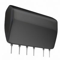
IC AC/DC CONV 12V 300MA SIP12
Manufacturer
Rohm Semiconductor
Series
BP5048r
Datasheet
1.BP5048.pdf
(4 pages)
Specifications of BP5048
Voltage - Output
12V
Number Of Outputs
1
Power (watts)
3W
Applications
Commercial
Power Supply Type
Switching (Closed Frame)
Voltage - Input
220VAC
Mounting Type
Through Hole
1st Output
12 VDC @ 300mA
Size / Dimension
1.38" L x 0.36" W x 0.87" H (35mm x 9.2mm x 22mm)
Power (watts) - Rated
3.6W
Operating Temperature
-20°C ~ 80°C
Efficiency
78%
Output Voltage
12 V
Input / Supply Voltage (max)
358 V
Input / Supply Voltage (min)
249 V
Operating Temperature Range
- 20 C to + 80 C
Mounting Style
Through Hole
Package / Case
SIP-12
Maximum Operating Temperature
+ 80 C
Minimum Operating Temperature
- 25 C
Output Current
300 mA
Lead Free Status / RoHS Status
Lead free / RoHS Compliant
Available stocks
Company
Part Number
Manufacturer
Quantity
Price


www.rohm.com
©2010 ROHM Co., Ltd. All rights reserved.
Non-Isolated AC/DC Converter
220VAC Input/12VDC (300mA) Output
BP5048
External Component Specifications
∗1 Maximum output current varies depending on ambient temperature ; please refer to derating curve.
∗2 Spike noise is not included in output ripple voltage.
Input voltage range
Output voltage
Output current
Line regulation
Load regulation
Output ripple voltage
Power conversion efficiency
Input voltage
Maximum output current
ESD endurance
Operating temperature range
Storage temperature range
Absolute Maximum Ratings
Electrical Characteristics
Application Circuit
FUSE: FUSE
C1: Input capacitor
C2: Output capacitor
C3: Noise removal capacitor
L1: Power inductor
D1: Rectifier diode
R1: Noise removal resistor
ZNR: Varistor
Vi
Please note that the input
side is at Pin 12.
BP5048
Parameter
Please verify operation and characteristics in the customer's circuit before actual usage.
Ensure that the load current does not exceed the maximum rating.
∼
Parameter
ZNR
D1
+
−
C1
Symbol
R1
Vo
Vp
Vr
Vi
Io
Vl
η
12
Use a fuse of 1A.
Rated voltage 450V or higher 22 to 820µF
Permissible ripple current 0.13Arms or higher
Rated voltage 25V or higher, 100 to 470µF
Low impedance type
Impedance is 0.4Ω max at high frequencies.
Evaluate under actual operating conditions.
Rated voltage 450V or higher 0.1 to 0.22µF
Film or ceramic capacitor
Evaluate under actual operating conditions.
Inductance = 1.0mH
Permissible current value 600mA or higher
Recommended part : C13-FR-GA (MITSUMI)
or TSL3135S-102JR78 (TDK)
A reverse surge voltage 600V or higher
An average rectifying current of 0.5A
The forward surge current should be 20A or higher.
10 to 22Ω 1/4W
Determine the ideal value through actual testing.
A varistor is required to protect against lightning surges and
static electricity.
FUSE
C3
Use a fuse for safety
−0.20
−0.20
10
11.0
Min.
249
65
0
−
Symbol
Vsurge
7
Iomax
Topr
Tstg
Vi
12.0
0.05
0.05
0.07
Typ.
311
78
5
−
1mH
L1
3
+
−
Max.
13.0
0.20
0.20
0.15
358
300
1
−
C2
Io
−25 to +105
−20 to +80
Limits
Vp-p
Unit
mA
358
300
%
V
V
V
V
2
Vo
1/1
DC
Vi=311V, Io=100mA
Vi=311V
Vi=249 to 358V, Io=100mA
Vi=311V, Io=0 to 100mA
Vi=311V, Io=100mA
Vi=311V, Io=300mA
Pin No.
10
11
12
1
2
3
4
5
6
7
8
9
Output terminal Vo(12V)
Skip
Choke coil connect
Skip
Choke coil connect
Skip
COMMON
Skip
Skip
N.C.
Skip
Input terminal Vi(311VDC)
Conditions
Function
mApk
Unit
kV
°C
°C
V
∗1
∗2
3 . 6 M A X
Dimensions (Unit : mm)
Derating Curve
Conversion Efficiency
Load Regulation
Surface Temperature Increase
100
13.0
12.8
12.6
12.4
12.2
12.0
11.8
11.6
11.4
11.2
350
300
250
200
150
100
90
80
70
60
50
40
30
20
10
50
40
35
30
25
20
15
10
0
-30 -20 -10
0
5
0
0
0
0
5 . 0 8
1
Ambient Temperature Ta ( °C )
50
50
Surface Temperature Increase
50
3
Output Current Io (mA)
Conversion Efficiency
Output Current Io (mA)
0 . 5 ± 0 . 1
(Ta=25 °C , Vi= 311 V)
Output Current Io (mA)
(Ta=25 °C , Vi=311V)
0 10
Data Sheet
2.54 � 11=27.94
Derating Curve
(Ta=25 °C , Vi=311V)
Operation Range
100
100
100
35.0MAX.
Load Regulation
5
20
7
150
2010.01 - Rev.A
150
150
7 . 6 2
1 . 3 ± 0 . 2
30
40
200
1 0
200
200
50
60
1 2
250
250
250
0 . 2 5 ± 0 . 0 5
70
80
300
300
300
90
9.2MAX.
4.85MAX.
4.35MAX.
Related parts for BP5048
Image
Part Number
Description
Manufacturer
Datasheet
Request
R

Part Number:
Description:
Manufacturer:
Rohm Semiconductor
Datasheet:
Part Number:
Description:
Manufacturer:
Rohm Semiconductor
Datasheet:
Part Number:
Description:
Manufacturer:
Rohm Semiconductor
Datasheet:
Part Number:
Description:
Manufacturer:
Rohm Semiconductor
Datasheet:
Part Number:
Description:
Manufacturer:
Rohm Semiconductor
Datasheet:
Part Number:
Description:
Manufacturer:
Rohm Semiconductor
Datasheet:
Part Number:
Description:
Manufacturer:
Rohm Semiconductor
Datasheet:
Part Number:
Description:
Manufacturer:
Rohm Semiconductor
Datasheet:
Part Number:
Description:
Manufacturer:
Rohm Semiconductor
Datasheet:
Part Number:
Description:
Manufacturer:
Rohm Semiconductor
Datasheet:
Part Number:
Description:
Manufacturer:
Rohm Semiconductor
Datasheet:
Part Number:
Description:
Manufacturer:
Rohm Semiconductor
Datasheet:

Part Number:
Description:
DIODE SWITCH 80V 25MA SMD5 TR
Manufacturer:
Rohm Semiconductor
Datasheet:
BP5048 Summary of contents
Page 1
... Vl Output ripple voltage − Vp Power conversion efficiency η 65 ∗1 Maximum output current varies depending on ambient temperature ; please refer to derating curve. ∗2 Spike noise is not included in output ripple voltage. Application Circuit BP5048 Please note that the input side is at Pin 12 FUSE ZNR C1 ∼ ...
Page 2
...
Page 3
...
Page 4
No copying or reproduction of this document, in part or in whole, is permitted without the consent of ROHM Co.,Ltd. The content specified herein is subject to change for improvement without notice. The content specified herein is for the purpose ...