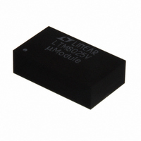
LTM8025EV#PBF Linear Technology, LTM8025EV#PBF Datasheet - Page 12

LTM8025EV#PBF
Manufacturer Part Number
LTM8025EV#PBF
Description
IC CONVERTER BUCK 3A ADJ 70LGA
Manufacturer
Linear Technology
Series
µModuler
Type
Point of Load (POL) Non-Isolatedr
Datasheet
1.LTM8025EVPBF.pdf
(20 pages)
Specifications of LTM8025EV#PBF
Design Resources
LTM8025 Spice Model
Output
0.8 ~ 24 V
Number Of Outputs
1
Power (watts)
72W
Mounting Type
Surface Mount
Voltage - Input
3.6 ~ 36 V
Package / Case
70-LGA
1st Output
0.8 ~ 24 VDC @ 3A
Size / Dimension
0.59" L x 0.35" W x 0.17" H (15mm x 9mm x 4.32mm)
Power (watts) - Rated
72W
Operating Temperature
-40°C ~ 125°C
Lead Free Status / RoHS Status
Lead free / RoHS Compliant
3rd Output
-
2nd Output
-
Available stocks
Company
Part Number
Manufacturer
Quantity
Price
LTM8025
APPLICATIONS INFORMATION
Table 2. Switching Frequency vs R
Operating Frequency Tradeoffs
It is recommended that the user apply the optimal R
value given in Table 1 for the input and output operating
condition. System level or other considerations, however,
may necessitate another operating frequency. While the
LTM8025 is fl exible enough to accommodate a wide range
of operating frequencies, a haphazardly chosen one may
result in undesirable operation under certain operating or
fault conditions. A frequency that is too high can reduce
effi ciency, generate excessive heat or even damage the
LTM8025 if the output is overloaded or short circuited.
A frequency that is too low can result in a fi nal design
that has too much output ripple or too large of an output
capacitor.
BIAS Pin Considerations
The BIAS pin is used to provide drive power for the in-
ternal power switching stage and operate other internal
circuitry. For proper operation, it must be powered by at
least 2.8V. If the output voltage is programmed to 2.8V
or higher, BIAS may be simply tied to AUX. If V
than 2.8V, BIAS can be tied to V
source. If the BIAS pin voltage is too high, the effi ciency
of the LTM8025 may suffer. The optimum BIAS voltage is
12
SWITCHING FREQUENCY
0.2MHz
0.3MHz
0.4MHz
0.5MHz
0.6MHz
0.7MHz
0.8MHz
0.9MHz
1.2MHz
1.4MHz
1.6MHz
1.8MHz
2.2MHz
2.4MHz
1MHz
2MHz
T
Value
IN
or some other voltage
R
76.8kΩ
63.4kΩ
52.3kΩ
44.2kΩ
38.3kΩ
34.0kΩ
26.7kΩ
21.5kΩ
17.8kΩ
14.7kΩ
12.1kΩ
9.76kΩ
8.25kΩ
T
215kΩ
137kΩ
100kΩ
VALUE
OUT
is less
T
dependent upon many factors, such as load current, input
voltage, output voltage and switching frequency, but 4V to
5V works well in many applications. In all cases, ensure
that the maximum voltage at the BIAS pin is less than 25V
and that the sum of V
power is applied from a remote or noisy voltage source, it
may be necessary to apply a decoupling capacitor locally
to the pin.
Load Sharing
Two or more LTM8025’s may be paralleled to produce higher
currents. To do this, tie the V
pins of all the paralleled LTM8025’s together. To ensure
that paralleled modules start up together, the RUN/SS pins
may be tied together, as well. If the RUN/SS pins are not
tied together, make sure that the same valued soft-start
capacitors are used for each module. Current sharing can
be improved by synchronizing the LTM8025s. An example
of two LTM8025s confi gured for load sharing is given in
the Typical Applications section.
Burst Mode Operation
To enhance effi ciency at light loads, the LTM8025 auto-
matically switches to Burst Mode operation which keeps
the output capacitor charged to the proper voltage while
minimizing the input quiescent current. During Burst Mode
operation, the LTM8025 delivers single cycle bursts of
current to the output capacitor followed by sleep periods
where the output power is delivered to the load by the output
capacitor. In addition, V
each reduced to microamps during the sleep time. As the
load current decreases towards a no load condition, the
percentage of time that the LTM8025 operates in sleep
mode increases and the average input current is greatly
reduced, resulting in higher effi ciency.
Burst Mode operation is enabled by tying SYNC to GND. To
disable Burst Mode operation, tie SYNC to a stable voltage
above 0.7V. Do not leave the SYNC pin fl oating.
Minimum Input Voltage
The LTM8025 is a step-down converter, so a minimum
amount of headroom is required to keep the output in
regulation. In addition, the input voltage required to turn
IN
IN
and BIAS is less than 56V. If BIAS
and BIAS quiescent currents are
IN
, ADJ, V
OUT
and SHARE
8025fa


