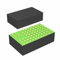
LTM8031IV#PBF Linear Technology, LTM8031IV#PBF Datasheet - Page 12

LTM8031IV#PBF
Manufacturer Part Number
LTM8031IV#PBF
Description
IC BUCK ADJ 1A 71LGA
Manufacturer
Linear Technology
Series
µModuler
Type
Point of Load (POL) Non-Isolatedr
Datasheet
1.LTM8031EVPBF.pdf
(20 pages)
Specifications of LTM8031IV#PBF
Design Resources
LTM8031 Spice Model
Output
0.8 ~ 10 V
Number Of Outputs
1
Power (watts)
10W
Mounting Type
Surface Mount
Voltage - Input
3.6 ~ 36 V
Package / Case
71-LGA
1st Output
0.8 ~ 10 VDC @ 1A
Size / Dimension
0.59" L x 0.35" W x 0.11" H (15mm x 9mm x 2.8mm)
Power (watts) - Rated
10W
Operating Temperature
-40°C ~ 125°C
Approvals
EN
Lead Free Status / RoHS Status
Lead free / RoHS Compliant
3rd Output
-
2nd Output
-
APPLICATIONS INFORMATION
LTM8031
Shorted Input Protection
Care needs to be taken in systems where the output will
be held high when the input to the LTM8031 is absent.
This may occur in battery charging applications or in
battery back-up systems where a battery or some other
supply is diode ORed with the LTM8031’s output. If the
V
(either by a logic signal or because it is tied to V
the LTM8031’s internal circuitry will pull its quiescent
current through its internal power switch. This is fi ne if
your system can tolerate a few milliamps in this state. If
you ground the RUN/SS pin, the internal switch current
will drop to essentially zero. However, if the V
grounded while the output is held high, then parasitic
diodes inside the LTM8031 can pull large currents from
the output through the V
device. Figure 2 shows a circuit that will run only when
the input voltage is present and that protects against a
shorted or reversed input.
PCB Layout
Most of the headaches associated with PCB layout have
been alleviated or even eliminated by the high level of
integration of the LTM8031. The LTM8031 is neverthe-
less a switching power supply and care must be taken to
minimize EMI and ensure proper operation. Even with the
high level of integration, you may fail to achieve specifi ed
12
IN
pin is allowed to fl oat and the RUN/SS pin is held high
IN
pin, potentially damaging the
Figure 2. The Input Diode Prevents a Shorted Input from Discharging
a Back-Up Battery Tied to the Output. It Also Protects the Circuit from
a Reversed Input. The LTM8031 Runs Only When the Input is Present
V
IN
IN
IN
), then
pin is
V
RUN/SS
IN
R
T
LTM8031
SYNC
operation with a haphazard or poor layout. See Figure 3
for a suggested layout.
Ensure that the grounding and heat sinking are acceptable.
A few rules to keep in mind are:
1. Place the R
2. Place the C
3. Place the C
4. Place the C
5. Connect all of the GND connections to as large a copper
6. Use vias to connect the GND copper area to the board’s
their respective pins.
and GND connection of the LTM8031. If a capacitor
is connected to the FIN terminals, place it as close
as possible to the FIN terminals, such that its ground
connection is as close as possible to that of the C
capacitor.
V
ground currents fl ow directly adjacent or underneath
the LTM8031.
pour or plane area as possible on the top layer. Avoid
breaking the ground connection between the external
components and the LTM8031.
internal ground plane. Liberally distribute these GND vias
to provide both a good ground connection and thermal
path to the internal planes of the printed circuit board.
GND
V
OUT
BIAS
AUX
ADJ
OUT
and GND connection of the LTM8031.
8031 F02
ADJ
IN
OUT
IN
V
capacitor as close as possible to the V
OUT
and R
and C
capacitor as close as possible to the
T
OUT
resistors as close as possible to
capacitors such that their
8031fa
IN
IN


