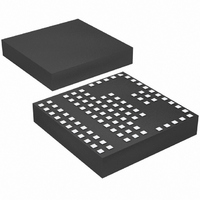
LTM4600IV#PBF Linear Technology, LTM4600IV#PBF Datasheet - Page 17

LTM4600IV#PBF
Manufacturer Part Number
LTM4600IV#PBF
Description
IC DC/DC UMODULE 10A 104-LGA
Manufacturer
Linear Technology
Series
µModuler
Type
Point of Load (POL) Non-Isolatedr
Datasheet
1.LTM4600EVPBF.pdf
(24 pages)
Specifications of LTM4600IV#PBF
Design Resources
LTM4600 Spice Model
Output
0.6 ~ 5 V
Number Of Outputs
1
Power (watts)
50W
Mounting Type
Surface Mount
Voltage - Input
4.5 ~ 20V
Package / Case
104-LGA
1st Output
0.6 ~ 5 VDC @ 10A
Size / Dimension
0.59" L x 0.59" W x 0.11" H (15mm x 15mm x 2.8mm)
Power (watts) - Rated
50W
Operating Temperature
-40°C ~ 85°C
Efficiency
92%
Lead Free Status / RoHS Status
Lead free / RoHS Compliant
3rd Output
-
2nd Output
-
Available stocks
Company
Part Number
Manufacturer
Quantity
Price
APPLICATIONS INFORMATION
The LTM4600 has a minimum (t
onds and a minimum (t
The 2.4V clamp on the ramp threshold as a function of
V
ratio of V
the fact the on time will not increase as V
past 2.4V. Therefore, if the nominal switching frequency
is 850kHz, then the switching frequency will increase
to ~1.2MHz for 3.3V, and ~1.7MHz for 5V outputs due
to Frequency = (DC/t
increases to 1.2MHz, then the time period t
to ~833 nanoseconds and at 1.7MHz the switching period
reduces to ~588 nanoseconds. When higher duty cycle
conversions like 5V to 3.3V and 12V to 5V need to be
accommodated, then the switching frequency can be
lowered to alleviate the violation of the 400ns minimum
off time. Since the total switching period is t
t
from the f
the on time generator, thus allowing for a longer on time
and a lower switching frequency. 12V to 5V and 5V to
3.3V derivations are explained in the data sheet to lower
switching frequency and accommodate these step-down
conversions.
Equations for setting frequency for 12V to 5V:
t
1MHz frequency or 1μs period is chosen for 12V to 5V.
OFF
OFF
OUT
I
frequency = (I
DC = duty cycle, duty cycle is (V
t
switching period; t
t
ON
S
ON
will be below the 400ns minimum off time. A resistor
must be greater than 400ns, or t
will cause the switching frequency to increase by the
= t
= (V
= DC • t
ON
OUT
ADJ
IN
+ t
Figure 17. LTM4600 Switching Period
/2.4V for 3.3V and 5V outputs. This is due to
– 0.7V)/110k; I
pin to ground can shunt current away from
S
OFF
(DC) DUTY CYCLE =
t
, t
OFF
ON
ON
PERIOD t
/[2.4V • 10pF]) • DC = 1.79MHz;
ON
S
OFF
= on-time, t
= 1/frequency
) When the switching frequency
s
) off time of 400 nanoseconds.
t
ON
t
ON
ON
t
s
ON
= 103μA
) on time of 100 nanosec-
4600 F21
DC =
FREQ =
OUT
OFF
S
t
ON
t
s
/V
t
DC
– t
ON
= off-time of the
=
V
IN
V
ON
OUT
IN
)
OUT
S
S
> 400ns.
= t
is reduced
increases
ON
+ t
OFF
,
t
band.
Using the frequency = (I
I
calculated from 12V input was 103μA, so a resistor from
f
57μA, sets the adequate I
range for the higher duty cycle conversion of 12V to
5V. Input voltage range is limited to 9V to 16V. Higher
input voltages can be used without the 15k on f
inductor ripple current gets too high above 16V, and the
400ns minimum off-time is limited below 9V.
Equations for setting frequency for 5V to 3.3V:
t
The ~450kHz frequency or 2.22μs period is chosen for
5V to 3.3V. Frequency range is about 450kHz to 650kHz
from 4.5V to 7V input.
t
band.
Using the frequency = (I
I
calculated from 5V input was 39μA, so a resistor from f
to ground = (0.7V/30.1k) = 23μA. 39μA – 23μA = 16μA,
sets the adequate I
for the higher duty cycle conversion of 5V to 3.3V. Input
voltage range is limited to 4.5V to 7V. Higher input voltages
can be used without the 30.1k on f
current gets too high above 7V, and the 400ns minimum
off-time is limited below 4.5V.
ON
ON
ADJ
OFF
ON
ON
t
t
I
frequency = (I
DC = duty cycle, duty cycle is (V
t
switching period; t
t
t
ON
OFF
ON
S
ON
OFF
and t
and t
= (450kHz • 2.4V • 10pF) • (1/0.66) ≅ 16μA. I
= (1MHz • 2.4V • 10pF) • (1/0.41) ≅ 58μA. I
must be greater than 400ns, or t
to ground = (0.7V/15k) = 46μA. 103μA – 46μA =
= t
= 0.41 • 1μs ≅ 410ns
= (V
= 0.66 • 2.22μs ≅ 1.46μs
= 1μs – 410ns ≅ 590ns
= 2.22μs – 1.46μs ≅ 760ns
OFF
ON
OFF
IN
are above the minimums with adequate guard
+ t
are above the minimums with adequate guard
– 0.7V)/110k; I
OFF
, t
ON
ON
ON
/[2.4V • 10pF]) • DC = 1.07MHz;
S
current for proper frequency range
= DC • t
= 1/frequency
ON
ON
ON
/[2.4V • 10pF]) • DC, solve for
/[2.4V • 10pF]) • DC, solve for
current for proper frequency
ON
= 39μA
S
, t
ADJ
OUT
OFF
. The inductor ripple
S
/V
– t
LTM4600
= off-time of the
IN
ON
)
> 400ns.
ON
ON
ADJ
17
current
current
. The
4600fc
ADJ


